X96012V14IZ Intersil, X96012V14IZ Datasheet - Page 18

X96012V14IZ
Manufacturer Part Number
X96012V14IZ
Description
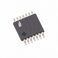
IC SENSOR CONDITION UNIV 14TSSOP
Manufacturer
Intersil
Type
Sensor Conditionerr
Datasheet
1.X96012V14IZT1.pdf
(23 pages)
Specifications of X96012V14IZ
Input Type
Voltage
Output Type
Voltage
Interface
2-Wire
Current - Supply
15mA
Mounting Type
Surface Mount
Package / Case
14-TSSOP
Lead Free Status / RoHS Status
Lead free / RoHS Compliant
Available stocks
Company
Part Number
Manufacturer
Quantity
Price
Part Number:
X96012V14IZ
Manufacturer:
INTERSIL
Quantity:
20 000
X96012 Memory Map
The X96012 contains a 2176 bit array of mixed volatile and
nonvolatile memory. This array is split up into four distinct
parts, namely: (Refer to Figure 15).
• General Purpose Memory (GPM)
• Look-up Table 1 (LUT1)
• Look-up Table 2 (LUT2)
• Control and Status Registers
The GPM is all nonvolatile EEPROM, located at memory
addresses 00h to 7Fh.
The Control and Status registers of the X96012 are used in
the test and setup of the device in a system. These registers
are realized as a combination of both volatile and nonvolatile
memory. These registers reside in the memory locations 80h
through 8Fh. The reserved bits within registers 80h through
86h, must be written as “0” if writing to them, and should be
ignored when reading. The reserved registers, from 88h
through 8Fh, must not be written, and their content should
be ignored.
ADDRESS
10FH
CFH
FFH
D0H
8FH
7FH
90H
80H
00H
SDA OUTPUT FROM
SDA OUTPUT FROM
7
FIGURE 15. X96012 MEMORY MAP
TRANSMITTER
SCL FROM
RECEIVER
CONTROL AND STATUS
MASTER
GENERAL PURPOSE
LOOK-UP TABLE 2
LOOK-UP TABLE 1
MEMORY (GPM)
REGISTERS
(LUT2)
(LUT1)
18
START
FIGURE 14. ACKNOWLEDGE RESPONSE FROM RECEIVER
0
64 BYTES
64 BYTES
16 BYTES
128 BYTES
SIZE
1
X96012
Both look-up tables LUT1 and LUT2 are realized as
non-volatile EEPROM, and extend from memory locations
90h - CFh and D0h - 10Fh respectively. These look-up tables
are dedicated to storing data solely for the purpose of setting
the outputs of Current Generators I1 and I2 respectively.
All bits in both look-up tables are preprogrammed to “0” at the
factory.
Addressing Protocol Overview
All Serial Interface operations must begin with a START,
followed by a Slave Address Byte. The Slave address
selects the X96012, and specifies if a Read or Write
operation is to be performed.
It should be noted that the Write Enable Latch (WEL) bit must
first be set in order to perform a Write operation to any other bit.
See “WEL: Write Enable Latch (Volatile)” on page 12. Also, all
communication to the X96012 over the 2-wire serial bus is
conducted by sending the MSB of each byte of data first.
Even though the 2176 bit memory consists of four differing
functions, it is physically realized as one contiguous array,
organized as 17 pages of 16 bytes each.
The X96012 2-wire protocol provides one address byte,
therefore, only 256 bytes can be addressed directly. The
next few sections explain how to access the different areas
for reading and writing.
SLAVE ADDRESS
SA7
1
SA7 - SA4
SA3 - SA1
BIT(S)
FIGURE 16. SLAVE ADDRESS (SA) FORMAT
DEVICE TYPE
SA0
SA6
IDENTIFIER
0
8
SA5
1
Device Type Identifier
Device Address
Read or Write Operation Select
SA4
0
ACK
SA3
AS2
9
ADDRESS
DESCRIPTION
DEVICE
SA2
AS1
AS0
SA1
READ OR
WRITE
R/W
February 20, 2008
SA0
FN8216.3


