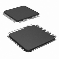
DS90CR484AVJD/NOPB National Semiconductor, DS90CR484AVJD/NOPB Datasheet

DS90CR484AVJD/NOPB
Specifications of DS90CR484AVJD/NOPB
Available stocks
Related parts for DS90CR484AVJD/NOPB
DS90CR484AVJD/NOPB Summary of contents
Page 1
... MHz and 8 serialized LVDS outputs are provided. Cable drive is enhanced with a user selectable Generalized Block Diagrams © 2008 National Semiconductor Corporation pre-emphasis feature that provides additional output current during transitions to counteract cable loading effects. Option balancing on a cycle-to-cycle basis, is also provided to reduce ISI (Inter-Symbol Interference) ...
Page 2
Generalized Transmitter Block Diagram Generalized Receiver Block Diagram Ordering Information Order Number DS90CR483AVJD DS90CR484AVJD www.national.com Function Transmitter (Serializer) Receiver (Deserializer) 2 30059202 30059203 Package VJD100A VJD100A ...
Page 3
... Absolute Maximum Ratings If Military/Aerospace specified devices are required, please contact the National Semiconductor Sales Office/ Distributors for availability and specifications. Supply Voltage ( CMOS/TTL Input Voltage LVCMOS/TTL Output −0. Voltage LVDS Receiver Input Voltage LVDS Driver Output Voltage LVDS Output Short Circuit Duration ...
Page 4
Symbol Parameter LVDS DRIVER DC SPECIFICATIONS |V | Differential Output OD Voltage ΔV Change in V between OD OD Complimentary Output States V Offset Voltage OS ΔV Change in V between OS OS Complimentary Output States I Output Short Circuit ...
Page 5
Transmitter Switching Characteristics Over recommended operating supply and temperature ranges unless otherwise specified. Symbol Parameter LLHT LVDS Low-to-High Transition Time, (Figure 2), PRE = 0.75V (disabled) LVDS Low-to-High Transition Time, (Figure 2), PRE = Vcc (max) LHLT LVDS High-to-Low Transition ...
Page 6
Chipset RSKM Characteristics Over recommended operating supply and temperature ranges unless otherwise specified.(Notes 4, 7). See Applications Informa- tion section for more details on this parameter and how to apply it. Symbol Parameter RSKM Receiver Skew Margin without Deskew in ...
Page 7
AC Timing Diagrams Note 9: The worst case test pattern produces a maximum toggling of digital circuits, LVDS I/O and CMOS/TTL I/O. FIGURE 2. DS90CR483A (Transmitter) LVDS Output Load and Transition Times FIGURE 3. DS90CR484A (Receiver) CMOS/TTL Output Load and ...
Page 8
FIGURE 5. DS90CR483A (Transmitter) Setup/Hold and High/Low Times FIGURE 6. DS90CR484A (Receiver) Setup/Hold and High/Low Times FIGURE 7. DS90CR483A (Transmitter) Propagation Delay - Latency www.national.com 30059215 30059216 30059227 8 ...
Page 9
FIGURE 8. DS90CR484A (Receiver) Propagation Delay - Latency FIGURE 9. DS90CR483A (Transmitter) Phase Lock Loop Set Time FIGURE 10. DS90CR484A (Receiver) Phase Lock Loop Set Time 9 30059228 30059219 30059220 www.national.com ...
Page 10
FIGURE 11. DS90CR483A (Transmitter) Power Down Delay FIGURE 12. DS90CR484A (Receiver) Power Down Delay www.national.com 30059221 30059222 10 ...
Page 11
C — Setup and Hold Time (Internal data sampling window) defined by Rspos (receiver input strobe position) min and max TPPOS — Transmitter output pulse position (min and max) ≥ RSKM Cable Skew (type, length) + LVDS Source Clock Jitter ...
Page 12
LVDS Interface Optional features supported: Pre-emphasis, and Deskew FIGURE 15. 48 Parallel TTL Data Bits Mapped to LVDS Outputs with DC Balance Enabled www.national.com 12 30059204 ...
Page 13
Optional feature supported: Pre-emphasis FIGURE 16. 48 Parallel TTL Data Bits Mapped to LVDS Outputs with DC Balance Disabled 13 30059205 www.national.com ...
Page 14
Applications Information The DS90CR483A and DS90CR484A are upgrades to the DS90CR483 and DS90CR484. DS90CR484A no longer have a PLL auto gear option se- lectable via the PLLSEL pin. The PLLSEL pin now allows for the PLL low gear only or ...
Page 15
If the running word disparity is negative and the current data dis- parity is positive, the data shall be sent unmodified. If the running word disparity is negative and ...
Page 16
HOW TO CONFIGURE FOR CABLE INTERCONNECT APPLICATIONS In applications that require the long cable drive capability. The DS90CR483A/DS90CR484A chipset is improved over prior generations of ...
Page 17
... Typical Data Rate vs Cable Length Curve DATA RATE VS CABLE LENGTH TEST PROCEDURE The Data Rate vs Cable Length graph was generated using National Semiconductor’s CLINK3V48BT-112 Evaluation Kit and 3M’s Mini D Ribbon (MDR) Cable under typical conditions (Vcc = 3.3V, Temp = +25°C). A Tektronix MB100 Bit-Error-Rate Tester (BERT) ...
Page 18
DS90CR483A Pin Descriptions—Channel Link Transmitter Pin Name I/O TxIN I TxOUTP O TxOUTM O TxCLKIN I TxCLKP O TxCLKM PLLSEL I PRE I DS_OPT I BAL GND I PLLV I CC PLLGND I ...
Page 19
DS90CR484A Pin Descriptions—Channel Link Receiver Pin Name I/O RxINP I Positive LVDS differential data inputs. RxINM I Negative LVDS differential data inputs. RxOUT O TTL level data outputs. In PowerDown (PD = Low) mode, receiver outputs are forced to a ...
Page 20
Pin Diagram www.national.com Transmitter - DS90CR483A - TQFP (TOP VIEW) 20 30059206 ...
Page 21
Pin Diagram Receiver - DS90CR484A - TQFP (TOP VIEW) 21 30059207 www.national.com ...
Page 22
Physical Dimensions Order Number DS90CR483AVJD and DS90CR484AVJD www.national.com inches (millimeters) unless otherwise noted Dimensions show in millimeters NS Package Number VJD100A 22 ...
Page 23
Notes 23 www.national.com ...
Page 24
... For more National Semiconductor product information and proven design tools, visit the following Web sites at: Products Amplifiers www.national.com/amplifiers Audio www.national.com/audio Clock Conditioners www.national.com/timing Data Converters www.national.com/adc Displays www.national.com/displays Ethernet www.national.com/ethernet Interface www.national.com/interface LVDS www.national.com/lvds Power Management www.national.com/power Switching Regulators www.national.com/switchers LDOs www ...


