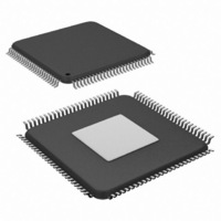
SCAN25100TYA/NOPB National Semiconductor, SCAN25100TYA/NOPB Datasheet - Page 15

SCAN25100TYA/NOPB
Manufacturer Part Number
SCAN25100TYA/NOPB
Description
IC SERIAL/DESERIAL CPRI 100-TQFP
Manufacturer
National Semiconductor
Series
SCANr
Datasheet
1.SCAN25100TYANOPB.pdf
(34 pages)
Specifications of SCAN25100TYA/NOPB
Function
Serializer/Deserializer
Data Rate
2.5Gbps
Input Type
LVTTL/LVCMOS
Output Type
LVTTL, LVCMOS
Number Of Inputs
10
Number Of Outputs
10
Voltage - Supply
1.7 V ~ 1.9 V
Operating Temperature
-40°C ~ 85°C
Mounting Type
Surface Mount
Package / Case
100-TQFP Exposed Pad, 100-eTQFP, 100-HTQFP, 100-VQFP
Operating Temperature (min)
-40C
Operating Temperature Classification
Industrial
Operating Temperature (max)
85C
Package Type
TQFP EP
Rad Hardened
No
Lead Free Status / RoHS Status
Lead free / RoHS Compliant
Other names
SCAN25100TYA
Available stocks
Company
Part Number
Manufacturer
Quantity
Price
Company:
Part Number:
SCAN25100TYA/NOPB
Manufacturer:
NS
Quantity:
158
Company:
Part Number:
SCAN25100TYA/NOPB
Manufacturer:
Texas Instruments
Quantity:
10 000
stant and these and other system delays can be measured
using DCM.
SYSCLK can be used to synchronize remote radio heads
since it provides a local 30.72 MHz internal clock which is
gracefully transitioned to the recovered clock. RXCLK is dig-
ital and synchronous to recovered output data and its phase
versus the incoming serial stream can be precisely measured
using DCM. Either or both recovered clocks may be used de-
pending on application requirements.
SPMODE[1:0] SPEED RATE SELECTION
The SCAN25100 operates in from a constant 30.72 MHz RE-
FCLK clock and performs necessary clock multiplication in-
ternally to support CPRI base station data rates. The speed
VSEL PIN 1.8CMOS/3.3LVTTL SELECT
The parallel input bus, output bus, and control pins are con-
figurable for either 1.8V CMOS or 3.3V LVTTL compliance.
RXCLK (write mode)
SYSCLK
BTS SerDes Mode (OPMODE = 0)
0 (BTS Mode)
0 (BTS Mode)
0 (BTS Mode)
0 (BTS Mode)
OPMODE
1.8V CMOS
3.3V LVCMOS
Pin
Compliance
REFCLK Mode
1.8V CMOS or
SPMODE[1]
LVTTL
Tie to ground
Tie to IOVDD supply (must power up with IOVDD)
LVDS
Type
0
0
1
1
TABLE 4. Speed Rate Configuration Truth Table
TABLE 3. Reference Clock Input Requirements
FIGURE 3. SCAN25100 REFCLK Termination
TABLE 2. Recovered Clock Truth Table
(internal oscillator)
30.72 MHz ± 5%
TABLE 5. VSEL Pin Control Options
Before Lock
Clock Rate
SPMODE[0]
30.72 MHz
High-Z
VSEL Control Pin
0
1
0
1
15
Duty Cycle
40% / 60%
Digital recovered clock
synchronous to output data
30.72 MHz analog recovered
clock from deserializer PLL
SYSCLK AND RXCLK RECOVERED CLOCKS
The SCAN25100 provides two recovered clocks, RXCLK (in
write mode) and SYSCLK, with different characteristics:
REFERENCE CLOCK
The differential REFCLKP and REFCLKN input impedance
accepts LVDS or LVPECL level signals. These pins should
be terminated with appropriate surface mount resistor(s)
placed close to the REFCLKP and REFCLKN inputs.
rate is programmable using the SPMODE[1:0] pins or through
MDIO when SPMODE[1:0] are pulled low. MDIO default
speed is 1228.8 Mbps on initial power up or reset.
To ensure reliable device operation, the VSEL and IOVDD
must be configured properly:
30.72 MHz
30.72 MHz
30.72 MHz
30.72 MHz
REFCLK
After Lock
Accuracy
±100 ppm
TXCLK/RXCLK
122.88 MHz
30.72 MHz
61.44 MHz
Reserved
1.8V
3.3V
IOVDD Supply Pins
Can be measured via DCM
Not Specified
Jitter (Typ)
40 ps p-p
Phase vs. Incoming Serial
1228.8 Mbps
2457.6 Mbps
Serial Rate
614.4 Mbps
Stream
Reserved
20183470
Jitter (Max)
140 ps p-p
www.national.com


