SCAN25100TYA/NOPB National Semiconductor, SCAN25100TYA/NOPB Datasheet - Page 5

SCAN25100TYA/NOPB
Manufacturer Part Number
SCAN25100TYA/NOPB
Description
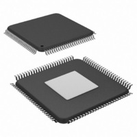
IC SERIAL/DESERIAL CPRI 100-TQFP
Manufacturer
National Semiconductor
Series
SCANr
Datasheet
1.SCAN25100TYANOPB.pdf
(34 pages)
Specifications of SCAN25100TYA/NOPB
Function
Serializer/Deserializer
Data Rate
2.5Gbps
Input Type
LVTTL/LVCMOS
Output Type
LVTTL, LVCMOS
Number Of Inputs
10
Number Of Outputs
10
Voltage - Supply
1.7 V ~ 1.9 V
Operating Temperature
-40°C ~ 85°C
Mounting Type
Surface Mount
Package / Case
100-TQFP Exposed Pad, 100-eTQFP, 100-HTQFP, 100-VQFP
Operating Temperature (min)
-40C
Operating Temperature Classification
Industrial
Operating Temperature (max)
85C
Package Type
TQFP EP
Rad Hardened
No
Lead Free Status / RoHS Status
Lead free / RoHS Compliant
Other names
SCAN25100TYA
Available stocks
Company
Part Number
Manufacturer
Quantity
Price
Company:
Part Number:
SCAN25100TYA/NOPB
Manufacturer:
NS
Quantity:
158
Company:
Part Number:
SCAN25100TYA/NOPB
Manufacturer:
Texas Instruments
Quantity:
10 000
MDC/MDIO
IEEE 1149.1 (JTAG)
RESERVED PINS
POWER
1, 2, 28, 29 PVDD33
GROUND
32, 38, 47,
50, 51, 76,
3, 4, 5, 10,
13, 16, 19,
24, 25, 26,
27, 39, 40,
48, 49, 63,
9, 15, 20,
8, 14, 21,
75, 86
Pin #
100
96
97
98
99
30
31
37
36
35
34
33
45
41
44
43
46
83
84
85
42
87
SPMODE [0]
SPMODE [1]
TENBMODE
LOOP [0]
LOOP [1]
MDC
MDIO
ADD0
ADD1
ADD2
ADD3
ADD4
TDI
TDO
TMS
TCK
TRSTB
RES1
RES2
AVDD18
AVDD33
IOVDD
GND
Pin Name
LVCMOS, Internal
LVCMOS, Internal
Internal pull up on
Internal pull up on
LVCMOS Internal
I, LVTTL or 1.8V
I, LVTTL or 1.8V
I, LVTTL or 1.8V
TDI, TMS, and
3.3V LVTTL
3.3V LVTTL
ADDR pins
I/O, Type
pull down
pull down
pull down
I, Ground
I, Power
I, Power
I, Power
I, Power
TRSTB
I
Speed mode configuration. (OPMODE must be low)
Pulling both pins low enables MDIO control.
SPMODE [1]
0
0
1
1
Enable 10-bit mode
0 = Selects 8-bit mode. Enables the internal 8b/10b encoder and decoder.
1 = Selects 10-bit mode. Bypasses internal 8b/10b encoder and decoder.
Loop back configuration.
Pulling both pins low enables MDIO control.
Note: During Special line (remote) loop back mode, the output de-emphasis control
is disabled.
LOOP [1]
0
0
1
1
MDC/MDIO configuration bus.
Protocol per IEEE 802.2ae-2002 MDC/MDIO Clause 45. These pins are 3.3V LVTTL
compatible, not 1.2V signal compatible.
JTAG test bus for IEEE 1149.1 and 1149.6 support.
Reserved.
Tie with 5 KΩ resistor to ground.
1.8V analog supply.
3.3V analog supply.
3.3V PLL supply (minimize supply noise to < 100 mV peak-to-peak).
1.8V or 3.3V parallel I/O bus and control pin supply.
See VSEL pin description for additional information.
Device ground.
The 8B/10B specification is defined in IEEE 802.3-2000 section 36.2.2
5
SPMODE [0]
0
1
0
1
LOOP [0]
0
1
0
1
Description
Rate selected via MDIO
614.4 Mbps rate mode
1228.8 Mbps rate mode
2457.6 Mbps rate mode
Normal mode—no loop back
Line (remote) loop back mode
Local loop back mode
Special line (remote) loop back mode
www.national.com


