CLC020BCQ/NOPB National Semiconductor, CLC020BCQ/NOPB Datasheet - Page 6
CLC020BCQ/NOPB
Manufacturer Part Number
CLC020BCQ/NOPB
Description
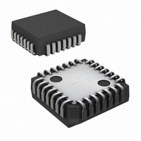
IC SERIALIZER VIDEO DGTL 28-PLCC
Manufacturer
National Semiconductor
Datasheet
1.CLC020BCQNOPB.pdf
(15 pages)
Specifications of CLC020BCQ/NOPB
Function
Serializer
Data Rate
400Mbps
Input Type
CMOS
Output Type
CMOS, TTL
Number Of Inputs
10
Number Of Outputs
1
Voltage - Supply
4.5 V ~ 5.5 V
Operating Temperature
0°C ~ 70°C
Mounting Type
Surface Mount
Package / Case
28-PLCC
For Use With
SD020EVK - BOARD EVALUATION CLC020
Lead Free Status / RoHS Status
Lead free / RoHS Compliant
Other names
*CLC020BCQ
*CLC020BCQ/NOPB
CLC020BCQ
*CLC020BCQ/NOPB
CLC020BCQ
Available stocks
Company
Part Number
Manufacturer
Quantity
Price
Company:

Part Number:
CLC020BCQ/NOPB
Manufacturer:
National Semiconductor
Quantity:
135
Company:
Part Number:
CLC020BCQ/NOPB
Manufacturer:
LT
Quantity:
4 067
Company:
Part Number:
CLC020BCQ/NOPB
Manufacturer:
Texas Instruments
Quantity:
10 000


www.national.com
Device Operation
The CLC020 SMPTE 259M Digital Video Serializer is used in
digital video signal origination and processing equipment:
cameras, video tape recorders, telecines, video test equip-
ment and others. It converts parallel component or compos-
ite digital video signals into serial format. Logic levels within
this equipment are normally TTL-compatible as produced by
CMOS or bipolar logic devices. The encoder outputs ECL-
compatible serial digital video (SDV) signals conforming to
SMPTE 259M-1997. The CLC020 operates at all standard
SMPTE and ITU-R parallel data rates.
VIDEO DATA PROCESSING CIRCUITS
The input data register accepts 8 or 10-bit parallel data and
clock signals having CMOS/TTL-compatible signal levels.
Parallel data may conform to any of several standards:
SMPTE 125M, SMPTE 267M, SMPTE 244M or ITU-R
BT.601. If data is 8-bit, it is converted to a 10-bit represen-
tation according to the type of data being input: component
4:2:2 per SMPTE 259M paragraph 7.1.1, composite NTSC
per paragraph 8.1.1 or composite PAL per paragraph 9.1.1.
Output from this register feeds the SMPTE polynomial
generator/serializer and sync detector. All CMOS inputs in-
cluding the P
The sync detector or TRS character detector accepts data
from the input register. The detection function is controlled
by Sync Detect Enable, a low-true, TTL-compatible, external
signal. Synchronization words, the timing reference signals
(TRS), start-of-active-video (SAV) and end-of-active-video
(EAV) are defined in SMPTE 125M-1995 and 244M. The
sync detector supplies control signals to the SMPTE polyno-
mial generator that identify the presence of valid video data.
The sync detector performs input TRS character LSB-
clipping as prescribed in ITU-R-BT.601. LSB-clipping causes
all TRS characters with a value between 000h and 003h to
be forced to 000h and all TRS characters with a value
between 3FCh and 3FFh to be forced to 3FFh. Clipping is
done prior to encoding.
The SMPTE polynomial generator accepts the parallel
video data and encodes it using the polynomial X
specified in SMPTE 259M–1997, paragraph 5 and Annex C.
The scrambled data is then serialized for output.
The NRZ-to-NRZI converter accepts serial NRZ data from
the SMPTE polynomial genertor and converts it to NRZI
using the polynomial X + 1 per SMPTE 259M–1997, para-
graph 5.2 and Annex C. The transmission bit order is LSB
first, per paragraph 6. The converter’s output feeds the
output driver amplifier.
CLK
input have internal pull-down devices.
FIGURE 4. Power-On Reset Sequence
9
+X
4
+1 as
6
PHASE-LOCKED LOOP AND VCO
The phase-locked loop (PLL) system generates the output
serial data clock at 10x the parallel data clock frequency.
This system consists of a VCO, divider chain, phase-
frequency detector and internal loop filter. The VCO free-
running frequency is internally set. The PLL automatically
generates the appropriate frequency for the serial clock rate
using the parallel data clock (P
ence. Loop filtering is internal to the CLC020. The VCO has
separate V
16, which may be supplied power independently via an
external low-pass filter, if desired. The PLL acquisition (lock)
time is less than 75 µs
LOCK DETECT
The Lock Detect output of the phase-frequency detector
indicates the PLL lock condition. It is a logic HIGH when the
loop is locked. The output is CMOS/TTL-compatible and is
suitable for driving other CMOS devices or a LED indicator.
SERIAL DATA OUTPUT BUFFER
The current-mode serial data outputs provide low-skew
complimentary or differential signals. The output buffer de-
sign can drive 75Ω coaxial cables (AC-coupled) or 10k/100k
ECL/PECL-compatible devices (DC-coupled). Output levels
are 800 mV
loads. The output level is 400 mV
coupled into 75Ω (See Application Information for details).
The 75Ω resistors connected to the SDO outputs are back-
matching resistors. No series back-matching resistors
should be used. SDO output levels are controlled by the
value of R
normally 1.69 kΩ,
device is in an out-of-lock condition. Separate V
V
serial output driver.
POWER-ON RESET
The CLC020 has an internally controlled, automatic,
power-on reset circuit. This circuit clears TRS detection
circuitry, all latches, registers, counters and polynomial gen-
erators and disables the serial output. The SDO outputs are
tri-stated during power-on reset. The part will remain in the
reset condition until the parallel input clock is applied.
It is recommended that P
30 µs after power has reached V
DDSD
power feeds, pins 21 and 24, are provided for the
REF
SSO
P-P
connected to pin 19. The value of R
and V
±
10% into 75Ω AC-coupled, back-matched
±
1%. The output buffer is static when the
DDO
@
270 Mbps.
CLK
power supply feeds, pins 15 and
not be asserted until at least
CLK
DD
) frequency as its refer-
10091714
min. See Figure 4.
P-P
±
10% when DC-
SSSD
REF
and
is
Related parts for CLC020BCQ/NOPB
Image
Part Number
Description
Manufacturer
Datasheet
Request
R

Part Number:
Description:
Buffer / Driver / Receiver Logic IC
Manufacturer:
National Semiconductor

Part Number:
Description:
BOARD EVALUATION CLC020
Manufacturer:
National Semiconductor
Datasheet:
Part Number:
Description:
National Semiconductor [8-Bit D/A Converter]
Manufacturer:
National Semiconductor
Datasheet:
Part Number:
Description:
National Semiconductor [Media Coprocessor]
Manufacturer:
National Semiconductor
Datasheet:
Part Number:
Description:
Digitally Controlled Tone and Volume Circuit with Stereo Audio Power Amplifier, Microphone Preamp Stage and National 3D Sound
Manufacturer:
National Semiconductor
Datasheet:
Part Number:
Description:
Digitally Controlled Tone and Volume Circuit with Stereo Audio Power Amplifier, Microphone Preamp Stage and National 3D Sound
Manufacturer:
National Semiconductor
Datasheet:
Part Number:
Description:
AC97 Rev 2 Codec with Sample Rate Conversion and National 3D Sound
Manufacturer:
National Semiconductor
Part Number:
Description:
Manufacturer:
National Semiconductor
Datasheet:
Part Number:
Description:
Manufacturer:
National Semiconductor
Datasheet:
Part Number:
Description:
General Purpose, Low Voltage, Low Power, Rail-to-Rail Output Operational Amplifiers
Manufacturer:
National Semiconductor
Datasheet:
Part Number:
Description:
8-bit 20 MSPS flash A/D converter.
Manufacturer:
National Semiconductor
Datasheet:
Part Number:
Description:
Low Noise Quad Operational Amplifier
Manufacturer:
National Semiconductor
Datasheet:
Part Number:
Description:
Quad Differential Line Receivers
Manufacturer:
National Semiconductor
Datasheet:
Part Number:
Description:
Quad High Speed Trapezoidal? Bus Transceiver
Manufacturer:
National Semiconductor
Datasheet: