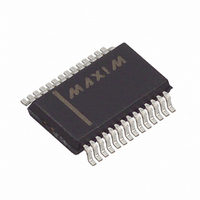
MAX9205EAI+ Maxim Integrated Products, MAX9205EAI+ Datasheet - Page 7

MAX9205EAI+
Manufacturer Part Number
MAX9205EAI+
Description
IC SERIALIZER LVDS 28-SSOP
Manufacturer
Maxim Integrated Products
Datasheet
1.MAX9205EAIT.pdf
(13 pages)
Specifications of MAX9205EAI+
Function
Serializer
Data Rate
400Mbps
Input Type
LVTTL/LVCMOS
Output Type
LVDS
Number Of Inputs
10
Number Of Outputs
1
Voltage - Supply
3 V ~ 3.6 V
Operating Temperature
-40°C ~ 85°C
Mounting Type
Surface Mount
Package / Case
28-SSOP
Input Current
+/- 20 uA
Input Voltage Range (max)
3.6 V
Interface Type
Parallel LVCMOS/LVTTL
Maximum Operating Temperature
+ 85 C
Minimum Operating Temperature
- 40 C
Mounting Style
SMD/SMT
Operating Supply Voltage
3.3 V
Settling Time
500 ps
Supply Voltage (max)
3.6 V
Supply Voltage (min)
3 V
Supply Voltage Range
3V To 3.6V
Operating Temperature Range
-40°C To +85��C
Digital Ic Case Style
SSOP
No. Of Pins
28
Filter Terminals
SMD
Control Interface
Serial
Supply Voltage Min
3V
Rohs Compliant
Yes
Data Rate Max
660Mbps
Lead Free Status / RoHS Status
Lead free / RoHS Compliant
Bypass AVCC with high-frequency surface-mount
ceramic 0.1µF and 0.001µF capacitors in parallel as
close to the device as possible, with the smaller valued
capacitor closest to AVCC. Bypass DVCC with high-fre-
quency surface-mount ceramic 0.1µF and 0.001µF
capacitors in parallel as close to the device as possi-
ble, with the smaller valued capacitor closest to DVCC.
Output trace characteristics affect the performance of
the MAX9205/MAX9207. Use controlled-impedance
media and terminate at both ends of the transmission
line in the media's characteristic impedance.
Termination with a single resistor at the end of a point-
to-point link typically provides acceptable performance.
However, the MAX9205/MAX9207 output levels are
specified for double-terminated point-to-point and mul-
tipoint applications. With a single 100Ω termination, the
output swing is larger.
Figure 1. Output Voltage Definitions
Figure 3. Input Clock Transition Time Requirement
Differential Traces and Termination
Applications Information
OUT+
OUT-
_______________________________________________________________________________________
V
OD
Power-Supply Bypassing
R
R
2
2
L
L
TCLK
V
OS
10%
90%
t
CLKT
10-Bit Bus LVDS Serializers
Avoid the use of unbalanced cables such as ribbon or
simple coaxial cable. Balanced cables such as twisted
pair offer superior signal quality and tend to generate
less EMI due to canceling effects. Balanced cables
tend to pick up noise as common mode, which is
rejected by a differential receiver.
Eliminate reflections and ensure that noise couples as
common mode by running the differential traces close
together. Reduce skew by matching the electrical
length of the traces. Excessive skew can result in a
degradation of magnetic field cancellation.
The differential output signals should be routed close to
each other to cancel their external magnetic field.
Maintain a constant distance between the differential
traces to avoid discontinuities in differential impedance.
Avoid 90° turns and minimize the number of vias to fur-
ther prevent impedance discontinuities.
Figure 2. Worst-Case I
EVEN IN_
ODD IN_
TCLK
t
CLKT
90%
10%
TCLK_R/F = LOW
0
3V
CC
Test Pattern
7


