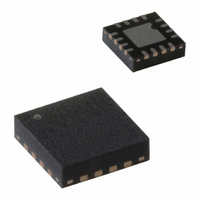
PCA9546ABS,118 NXP Semiconductors, PCA9546ABS,118 Datasheet - Page 14

PCA9546ABS,118
Manufacturer Part Number
PCA9546ABS,118
Description
IC I2C SWITCH 4CH 16-HVQFN
Manufacturer
NXP Semiconductors
Datasheet
1.PCA9546ABS118.pdf
(25 pages)
Specifications of PCA9546ABS,118
Package / Case
16-VQFN Exposed Pad, 16-HVQFN, 16-SQFN, 16-DHVQFN
Applications
4-Channel I²C Switcher
Interface
I²C, SMBus
Voltage - Supply
2.3 V ~ 5.5 V
Mounting Type
Surface Mount
Product
Multiplexer
Number Of Lines (input / Output)
4.0 / 1.0
Propagation Delay Time
0.3 ns at 2.3 V to 5.5 V
Supply Voltage (max)
5.5 V
Supply Voltage (min)
2.3 V
Maximum Operating Temperature
+ 85 C
Minimum Operating Temperature
- 40 C
Mounting Style
SMD/SMT
Number Of Input Lines
4.0
Number Of Output Lines
1.0
Lead Free Status / RoHS Status
Lead free / RoHS Compliant
Lead Free Status / RoHS Status
Lead free / RoHS Compliant, Lead free / RoHS Compliant
Other names
568-3378-2
935275811118
PCA9546ABS-T
935275811118
PCA9546ABS-T
Available stocks
Company
Part Number
Manufacturer
Quantity
Price
Part Number:
PCA9546ABS,118
Manufacturer:
NXP/恩智浦
Quantity:
20 000
NXP Semiconductors
Table 7.
V
[1]
[2]
PCA9546A_5
Product data sheet
Symbol
Supply
V
I
I
V
Input SCL; input/output SDA
V
V
I
I
I
C
Select inputs A0 to A2, RESET
V
V
I
C
Pass gate
R
V
I
C
DD
stb
OL
IL
IH
LI
L
SS
DD
POR
IL
IH
IL
IH
o(sw)
i
i
on
io
= 0 V; T
For operation between published voltage ranges, refer to the worst-case parameter in both ranges.
V
DD
must be lowered to 0.2 V in order to reset part.
Static characteristics at V
amb
Parameter
supply voltage
supply current
standby current
power-on reset voltage
LOW-level input voltage
HIGH-level input voltage
LOW-level output current
LOW-level input current
HIGH-level input current
input capacitance
LOW-level input voltage
HIGH-level input voltage
input leakage current
input capacitance
ON-state resistance
switch output voltage
leakage current
input/output capacitance
= 40 C to +85 C; unless otherwise specified. See
DD
Conditions
operating mode; V
no load; V
f
standby mode; V
no load; V
no load; V
V
V
V
V
V
pin at V
V
V
I
V
I
V
I
V
V
SCL
O
o(sw)
o(sw)
OL
OL
I
I
I
I
DD
i(sw)
i(sw)
I
I
= 4.5 V to 5.5 V
= V
= V
= V
= V
= 15 mA
= V
= V
= 0.4 V
= 0.6 V
= 100 kHz
= 4.5 V to 5.5 V; V
= 100 A
= 100 A
= V
= V
SS
DD
SS
SS
DD
SS
DD
DD
DD
or V
I
I
I
or V
Rev. 05 — 2 July 2009
= V
= V
= V
= 5.0 V;
= 4.5 V to 5.5 V;
SS
DD
DD
DD
SS
DD
or V
or V
or V
DD
= 5.5 V;
= 5.5 V;
SS
SS
SS
O
;
= 0.4 V;
Table 6 on page 13
[2]
4-channel I
Min
4.5
-
-
-
0.7V
3
6
-
0.7V
-
4
-
2.6
-
0.5
1
1
0.5
1
1
DD
DD
for V
DD
Typ
-
65
0.3
1.7
-
-
-
-
-
-
12
-
-
-
2
9
3.6
-
-
3
2
C-bus switch with reset
= 2.3 V to 3.6 V.
PCA9546A
© NXP B.V. 2009. All rights reserved.
Max
5.5
100
1
2.1
+0.3V
6
-
-
+1
+1
13
+0.3V
V
+1
3
24
-
4.5
+1
5
DD
+ 0.5
DD
DD
[1]
14 of 25
Unit
V
V
V
V
mA
mA
pF
V
V
pF
V
V
pF
A
A
A
A
A
A


