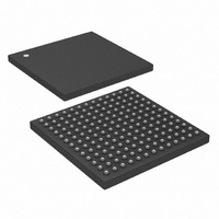
DS33Z11+ Maxim Integrated Products, DS33Z11+ Datasheet - Page 101

DS33Z11+
Manufacturer Part Number
DS33Z11+
Description
IC MAPPER ETHERNET 169-CSBGA
Manufacturer
Maxim Integrated Products
Datasheet
1.DS33Z11.pdf
(172 pages)
Specifications of DS33Z11+
Applications
Data Transport
Interface
SPI/Parallel
Voltage - Supply
1.8V, 3.3V
Package / Case
169-CSBGA
Mounting Type
Surface Mount
Lead Free Status / RoHS Status
Lead free / RoHS Compliant
- Current page: 101 of 172
- Download datasheet (2Mb)
9.5.5
Serial Receive Registers are used to control the HDLC Receiver associated with each Serial Interface. Note that
throughout this document HDLC Processor is also referred to as “Packet Processor”. The receive packet
processor block has seventeen registers.
9.5.5.1
Register Name:
Register Description:
Register Address:
Bit #
Name
Default
Bit 0: Receive Data Enable Polarity (RDENPLT) Receive Data Enable Polarity. If set to 1, RDEN Low enables
reception of the bit.
Register Name:
Register Description:
Register Address:
Bit #
Name
Default
Bit 5: Receive FCS Processing Disable (RFPD) – When equal to 0, FCS processing is performed and FCS is
appended to packets. When set to 1, FCS processing is disabled (the packets do not have an FCS appended). In
X.86 mode, FCS processing is always enabled.
Bit 4: Receive FCS-16 Enable (RF16) – When 0, the error checking circuit uses a 32-bit FCS. When 1, the error
checking circuit uses a 16-bit FCS. This bit is ignored when FCS processing is disabled. In X.86 mode, the FCS
is always 32 bits.
Bit 3: Receive FCS Extraction Disable (RFED) – When 0, the FCS bytes are discarded. When 1, the FCS bytes
are passed on. This bit is ignored when FCS processing is disabled. In X.86 mode, FCS bytes are discarded.
Bit 2: Receive Descrambling Disable (RDD) – When equal to 0, X
1, descrambling is disabled.
Bit 1: Receive Bit Reordering Enable (RBRE) – When equal to 0, reordering is disabled and the first bit
received is expected to be the MSB DT [7] of the byte. When set to 1, bit reordering is enabled and the first bit
received is expected to be the LSB DT [0] of the byte. Note that function is controlled by the BREO in Hardware
Mode.
Bit 0: Receive Clear Channel Enable (RCCE) – When equal to 0, packet processing is enabled. When set to 1,
the device is in clear channel mode and all packet-processing functions except descrambling and bit reordering
are disabled.
Receive Serial Interface
Register Bit Descriptions
7
0
7
0
-
-
6
0
6
0
-
-
LI.RSLCR
Receive Serial Interface Configuration Register
100h
LI.RPPCL
Receive Packet Processor Control Low Register
101h
RFPD
5
0
5
0
-
101 of 172
RF16
4
0
4
0
-
RFED
3
0
3
0
-
43
+1 descrambling is performed. When set to
RDD
2
0
2
0
-
RBRE
1
0
1
0
-
RDENPLT
RCCE
0
0
0
0
Related parts for DS33Z11+
Image
Part Number
Description
Manufacturer
Datasheet
Request
R

Part Number:
Description:
MAX7528KCWPMaxim Integrated Products [CMOS Dual 8-Bit Buffered Multiplying DACs]
Manufacturer:
Maxim Integrated Products
Datasheet:

Part Number:
Description:
Single +5V, fully integrated, 1.25Gbps laser diode driver.
Manufacturer:
Maxim Integrated Products
Datasheet:

Part Number:
Description:
Single +5V, fully integrated, 155Mbps laser diode driver.
Manufacturer:
Maxim Integrated Products
Datasheet:

Part Number:
Description:
VRD11/VRD10, K8 Rev F 2/3/4-Phase PWM Controllers with Integrated Dual MOSFET Drivers
Manufacturer:
Maxim Integrated Products
Datasheet:

Part Number:
Description:
Highly Integrated Level 2 SMBus Battery Chargers
Manufacturer:
Maxim Integrated Products
Datasheet:

Part Number:
Description:
Current Monitor and Accumulator with Integrated Sense Resistor; ; Temperature Range: -40°C to +85°C
Manufacturer:
Maxim Integrated Products

Part Number:
Description:
TSSOP 14/A�/RS-485 Transceivers with Integrated 100O/120O Termination Resis
Manufacturer:
Maxim Integrated Products

Part Number:
Description:
TSSOP 14/A�/RS-485 Transceivers with Integrated 100O/120O Termination Resis
Manufacturer:
Maxim Integrated Products

Part Number:
Description:
QFN 16/A�/AC-DC and DC-DC Peak-Current-Mode Converters with Integrated Step
Manufacturer:
Maxim Integrated Products

Part Number:
Description:
TDFN/A/65V, 1A, 600KHZ, SYNCHRONOUS STEP-DOWN REGULATOR WITH INTEGRATED SWI
Manufacturer:
Maxim Integrated Products

Part Number:
Description:
Integrated Temperature Controller f
Manufacturer:
Maxim Integrated Products

Part Number:
Description:
SOT23-6/I�/45MHz to 650MHz, Integrated IF VCOs with Differential Output
Manufacturer:
Maxim Integrated Products

Part Number:
Description:
SOT23-6/I�/45MHz to 650MHz, Integrated IF VCOs with Differential Output
Manufacturer:
Maxim Integrated Products

Part Number:
Description:
EVALUATION KIT/2.4GHZ TO 2.5GHZ 802.11G/B RF TRANSCEIVER WITH INTEGRATED PA
Manufacturer:
Maxim Integrated Products

Part Number:
Description:
QFN/E/DUAL PCIE/SATA HIGH SPEED SWITCH WITH INTEGRATED BIAS RESISTOR
Manufacturer:
Maxim Integrated Products
Datasheet:


