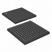
DS33Z11+ Maxim Integrated Products, DS33Z11+ Datasheet - Page 166

DS33Z11+
Manufacturer Part Number
DS33Z11+
Description
IC MAPPER ETHERNET 169-CSBGA
Manufacturer
Maxim Integrated Products
Datasheet
1.DS33Z11.pdf
(172 pages)
Specifications of DS33Z11+
Applications
Data Transport
Interface
SPI/Parallel
Voltage - Supply
1.8V, 3.3V
Package / Case
169-CSBGA
Mounting Type
Surface Mount
Lead Free Status / RoHS Status
Lead free / RoHS Compliant
- Current page: 166 of 172
- Download datasheet (2Mb)
Figure 12-2 TAP Controller State Diagram
12.2 Instruction Register
The instruction register contains a shift register as well as a latched parallel output and is 3 bits in length. When
the TAP controller enters the Shift-IR state, the instruction shift register is connected between JTDI and JTDO.
While in the Shift-IR state, a rising edge on JTCLK with JTMS LOW will shift the data one stage towards the serial
output at JTDO. A rising edge on JTCLK in the Exit1-IR state or the Exit2-IR state with JTMS HIGH will move the
controller to the Update-IR state. The falling edge of that same JTCLK will latch the data in the instruction shift
register to the instruction parallel output. Instructions supported by the DS33Z11 and its respective operational
binary codes are shown in
1
0
Test Logic
Reset
Run Test/
Idle
0
Table
1
12-1.
0
1
Capture DR
Update DR
1
Select
DR-Scan
Pause DR
Exit2 DR
Shift DR
Exit DR
0
1
0
0
1
0
1
166 of 172
1
0
0
1
0
1
Capture IR
Update IR
1
Pause IR
Select
IR-Scan
Shift IR
Exit2 IR
Exit IR
0
1
1
1
0
0
0
1
1
0
0
Related parts for DS33Z11+
Image
Part Number
Description
Manufacturer
Datasheet
Request
R

Part Number:
Description:
MAX7528KCWPMaxim Integrated Products [CMOS Dual 8-Bit Buffered Multiplying DACs]
Manufacturer:
Maxim Integrated Products
Datasheet:

Part Number:
Description:
Single +5V, fully integrated, 1.25Gbps laser diode driver.
Manufacturer:
Maxim Integrated Products
Datasheet:

Part Number:
Description:
Single +5V, fully integrated, 155Mbps laser diode driver.
Manufacturer:
Maxim Integrated Products
Datasheet:

Part Number:
Description:
VRD11/VRD10, K8 Rev F 2/3/4-Phase PWM Controllers with Integrated Dual MOSFET Drivers
Manufacturer:
Maxim Integrated Products
Datasheet:

Part Number:
Description:
Highly Integrated Level 2 SMBus Battery Chargers
Manufacturer:
Maxim Integrated Products
Datasheet:

Part Number:
Description:
Current Monitor and Accumulator with Integrated Sense Resistor; ; Temperature Range: -40°C to +85°C
Manufacturer:
Maxim Integrated Products

Part Number:
Description:
TSSOP 14/A�/RS-485 Transceivers with Integrated 100O/120O Termination Resis
Manufacturer:
Maxim Integrated Products

Part Number:
Description:
TSSOP 14/A�/RS-485 Transceivers with Integrated 100O/120O Termination Resis
Manufacturer:
Maxim Integrated Products

Part Number:
Description:
QFN 16/A�/AC-DC and DC-DC Peak-Current-Mode Converters with Integrated Step
Manufacturer:
Maxim Integrated Products

Part Number:
Description:
TDFN/A/65V, 1A, 600KHZ, SYNCHRONOUS STEP-DOWN REGULATOR WITH INTEGRATED SWI
Manufacturer:
Maxim Integrated Products

Part Number:
Description:
Integrated Temperature Controller f
Manufacturer:
Maxim Integrated Products

Part Number:
Description:
SOT23-6/I�/45MHz to 650MHz, Integrated IF VCOs with Differential Output
Manufacturer:
Maxim Integrated Products

Part Number:
Description:
SOT23-6/I�/45MHz to 650MHz, Integrated IF VCOs with Differential Output
Manufacturer:
Maxim Integrated Products

Part Number:
Description:
EVALUATION KIT/2.4GHZ TO 2.5GHZ 802.11G/B RF TRANSCEIVER WITH INTEGRATED PA
Manufacturer:
Maxim Integrated Products

Part Number:
Description:
QFN/E/DUAL PCIE/SATA HIGH SPEED SWITCH WITH INTEGRATED BIAS RESISTOR
Manufacturer:
Maxim Integrated Products
Datasheet:


