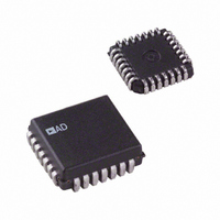
ADG407BPZ Analog Devices Inc, ADG407BPZ Datasheet - Page 3

ADG407BPZ
Manufacturer Part Number
ADG407BPZ
Description
IC MULTIPLEXER DUAL 8X1 28PLCC
Manufacturer
Analog Devices Inc
Series
LC²MOSr
Type
Analog Multiplexerr
Datasheet
1.ADG406BNZ.pdf
(20 pages)
Specifications of ADG407BPZ
Function
Multiplexer
Circuit
2 x 8:1
On-state Resistance
80 Ohm
Voltage Supply Source
Single Supply
Voltage - Supply, Single/dual (±)
5V, 12V
Current - Supply
100µA
Operating Temperature
-40°C ~ 85°C
Mounting Type
Surface Mount
Package / Case
28-LCC (J-Lead)
No. Of Circuits
2
Supply Current
100µA
On State Resistance Max
50ohm
Supply Voltage Range
10.8V To 13.2V, ± 13.5V To ± 16.5V
Operating Temperature Range
-40°C To +85°C
Multiplexer Configuration
Dual 8:1
Number Of Inputs
16
Number Of Outputs
2
Number Of Channels
2
Analog Switch On Resistance
125@10.8VOhm
Analog Switch Turn On Time
240ns
Analog Switch Turn Off Time
180ns
Package Type
PLCC
Power Supply Requirement
Single/Dual
Single Supply Voltage (typ)
12V
Single Supply Voltage (max)
25V
Dual Supply Voltage (typ)
±15V
Dual Supply Voltage (max)
±22V
Mounting
Surface Mount
Pin Count
28
Operating Temp Range
-40C to 85C
Operating Temperature Classification
Industrial
Package
28PLCC
Maximum On Resistance
125@10.8V Ohm
Maximum Propagation Delay Bus To Bus
150@±15V|220@12V ns
Maximum High Level Output Current
20 mA
Multiplexer Architecture
8:1
Maximum Turn-off Time
180@12V ns
Maximum Turn-on Time
240@12V ns
Power Supply Type
Single|Dual
Lead Free Status / RoHS Status
Lead free / RoHS Compliant
Lead Free Status / RoHS Status
Lead free / RoHS Compliant, Lead free / RoHS Compliant
Available stocks
Company
Part Number
Manufacturer
Quantity
Price
Company:
Part Number:
ADG407BPZ
Manufacturer:
Analog Devices Inc
Quantity:
10 000
Part Number:
ADG407BPZ
Manufacturer:
ADI/亚德诺
Quantity:
20 000
GENERAL DESCRIPTION
The ADG406, ADG407, and ADG426 are monolithic CMOS
analog multiplexers. The ADG406 and ADG426 switch one of
sixteen inputs to a common output as determined by the 4-bit
binary address lines: A0, A1, A2, and A3. The ADG426 has
on-chip address and control latches that facilitate microprocessor
interfacing. The ADG407 switches one of eight differential
inputs to a common differential output as determined by the
3-bit binary address lines A0, A1 and A2. An EN input on all
devices is used to enable or disable the device. When disabled,
all channels are switched off.
Rev. B | Page 3 of 20
The ADG406/ADG407/ADG426 are designed on an enhanced
LC
high switching speed and low on resistance. These features make
the parts suitable for high speed data acquisition systems and
audio signal switching. Low power dissipation makes the parts
suitable for battery powered systems. Each channel conducts
equally well in both directions when on and has an input signal
range which extends to the supplies. In the off condition, signal
levels up to the supplies are blocked. All channels exhibit break-
before-make switching action preventing momentary shorting
when switching channels. Inherent in the design is low charge
injection for minimum transients when switching the digital
inputs.
2
MOS process that provides low power dissipation yet gives
ADG406/ADG407/ADG426


