DS10CP152TMA/NOPB National Semiconductor, DS10CP152TMA/NOPB Datasheet - Page 4
DS10CP152TMA/NOPB
Manufacturer Part Number
DS10CP152TMA/NOPB
Description
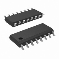
IC SW XPT 1.5GPS 2X2 LVDS 16SOIC
Manufacturer
National Semiconductor
Datasheet
1.DS10CP152TMANOPB.pdf
(12 pages)
Specifications of DS10CP152TMA/NOPB
Function
Crosspoint Switch
Circuit
1 x 2:2
Voltage Supply Source
Single Supply
Voltage - Supply, Single/dual (±)
3 V ~ 3.6 V
Current - Supply
58mA
Operating Temperature
-40°C ~ 85°C
Mounting Type
Surface Mount
Package / Case
16-SOIC (0.154", 3.90mm Width)
Supply Voltage Range
3V To 3.6V
Digital Ic Case Style
SOIC
No. Of Pins
16
Operating Temperature Range
-40°C To +85°C
Svhc
No SVHC (15-Dec-2010)
Base Number
10
Data Rate
1.5Gbps
Interface
LVDS
Rohs Compliant
Yes
Lead Free Status / RoHS Status
Lead free / RoHS Compliant
Other names
DS10CP152TMA
Available stocks
Company
Part Number
Manufacturer
Quantity
Price
Company:

Part Number:
DS10CP152TMA/NOPB
Manufacturer:
National Semiconductor
Quantity:
135


www.national.com
LVDS OUTPUT DC SPECIFICATIONS
V
ΔV
V
ΔV
I
C
R
SUPPLY CURRENT
I
I
Symbol
OS
CC
CCZ
OD
OS
OUT
OUT
Note 4: “Absolute Maximum Ratings” indicate limits beyond which damage to the device may occur, including inoperability and degradation of device reliability
and/or performance. Functional operation of the device and/or non-degradation at the Absolute Maximum Ratings or other conditions beyond those indicated in
the Recommended Operating Conditions is not implied. The Recommended Operating Conditions indicate conditions at which the device is functional and the
device should not be operated beyond such conditions.
Note 5: The Electrical Characteristics tables list guaranteed specifications under the listed Recommended Operating Conditions except as otherwise modified
or specified by the Electrical Characteristics Conditions and/or Notes. Typical specifications are estimations only and are not guaranteed.
Note 6: Current into device pins is defined as positive. Current out of device pins is defined as negative. All voltages are referenced to ground except V
ΔV
Note 7: Typical values represent most likely parametric norms for V
product characterization and are not guaranteed.
Note 8: Output short circuit current (I
OD
OS
OD
.
Differential Output Voltage
Change in Magnitude of V
Output States
Offset Voltage
Change in Magnitude of V
Output States
Output Short Circuit Current (Note 8)
Output Capacitance
Output Termination Resistor
Supply Current
Outputs Powered Down Supply Current
Parameter
OS
) is specified as magnitude only, minus sign indicates direction only.
OD
OS
for Complimentary
for Complimentary
CC
= +3.3V and T
R
R
OUT to GND
OUT to V
Any LVDS Output Pin to GND
Between OUT+ and OUT-
EN0 = EN1 = H
EN0 = EN1 = L
L
L
= 100Ω
= 100Ω
4
A
CC
= +25°C, and at the Recommended Operation Conditions at the time of
Conditions
1.05
Min
250
-35
-35
Typ
350
100
1.2
-23
1.2
58
25
8
1.375
Max
450
-55
35
35
55
70
30
OD
Units
and
mV
mV
mV
mA
mA
mA
mA
pF
Ω
V
Related parts for DS10CP152TMA/NOPB
Image
Part Number
Description
Manufacturer
Datasheet
Request
R

Part Number:
Description:
National Semiconductor [8-Bit D/A Converter]
Manufacturer:
National Semiconductor
Datasheet:
Part Number:
Description:
National Semiconductor [Media Coprocessor]
Manufacturer:
National Semiconductor
Datasheet:
Part Number:
Description:
Digitally Controlled Tone and Volume Circuit with Stereo Audio Power Amplifier, Microphone Preamp Stage and National 3D Sound
Manufacturer:
National Semiconductor
Datasheet:
Part Number:
Description:
Digitally Controlled Tone and Volume Circuit with Stereo Audio Power Amplifier, Microphone Preamp Stage and National 3D Sound
Manufacturer:
National Semiconductor
Datasheet:
Part Number:
Description:
AC97 Rev 2 Codec with Sample Rate Conversion and National 3D Sound
Manufacturer:
National Semiconductor
Part Number:
Description:
Manufacturer:
National Semiconductor
Datasheet:
Part Number:
Description:
Manufacturer:
National Semiconductor
Datasheet:
Part Number:
Description:
General Purpose, Low Voltage, Low Power, Rail-to-Rail Output Operational Amplifiers
Manufacturer:
National Semiconductor
Datasheet:
Part Number:
Description:
8-bit 20 MSPS flash A/D converter.
Manufacturer:
National Semiconductor
Datasheet:
Part Number:
Description:
Low Noise Quad Operational Amplifier
Manufacturer:
National Semiconductor
Datasheet:
Part Number:
Description:
Quad Differential Line Receivers
Manufacturer:
National Semiconductor
Datasheet:
Part Number:
Description:
Quad High Speed Trapezoidal? Bus Transceiver
Manufacturer:
National Semiconductor
Datasheet:
Part Number:
Description:
Dual Line Receiver
Manufacturer:
National Semiconductor
Datasheet:
Part Number:
Description:
TTL to 10k ECL Level Translator with Latch
Manufacturer:
National Semiconductor
Datasheet: