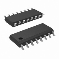
DS10CP152TMA/NOPB National Semiconductor, DS10CP152TMA/NOPB Datasheet - Page 5

DS10CP152TMA/NOPB
Manufacturer Part Number
DS10CP152TMA/NOPB
Description
IC SW XPT 1.5GPS 2X2 LVDS 16SOIC
Manufacturer
National Semiconductor
Datasheet
1.DS10CP152TMANOPB.pdf
(12 pages)
Specifications of DS10CP152TMA/NOPB
Function
Crosspoint Switch
Circuit
1 x 2:2
Voltage Supply Source
Single Supply
Voltage - Supply, Single/dual (±)
3 V ~ 3.6 V
Current - Supply
58mA
Operating Temperature
-40°C ~ 85°C
Mounting Type
Surface Mount
Package / Case
16-SOIC (0.154", 3.90mm Width)
Supply Voltage Range
3V To 3.6V
Digital Ic Case Style
SOIC
No. Of Pins
16
Operating Temperature Range
-40°C To +85°C
Svhc
No SVHC (15-Dec-2010)
Base Number
10
Data Rate
1.5Gbps
Interface
LVDS
Rohs Compliant
Yes
Lead Free Status / RoHS Status
Lead free / RoHS Compliant
Other names
DS10CP152TMA
Available stocks
Company
Part Number
Manufacturer
Quantity
Price
Company:
Part Number:
DS10CP152TMA/NOPB
Manufacturer:
National Semiconductor
Quantity:
135
LVDS OUTPUT AC SPECIFICATIONS
t
t
t
t
t
t
t
t
t
t
JITTER PERFORMANCE (Note 11)
t
t
t
t
t
t
t
t
t
t
t
t
PLHD
PHLD
SKD1
SKD2
SKD3
LHT
HLT
ON
OFF
SEL
RJ1
RJ2
RJ3
RJ4
DJ1
DJ2
DJ3
DJ4
TJ1
TJ2
TJ3
TJ4
AC Electrical Characteristics
Over recommended operating supply and temperature ranges unless otherwise specified. (Notes 9, 10)
Note 9: The Electrical Characteristics tables list guaranteed specifications under the listed Recommended Operating Conditions except as otherwise modified
or specified by the Electrical Characteristics Conditions and/or Notes. Typical specifications are estimations only and are not guaranteed.
Note 10: Typical values represent most likely parametric norms for V
product characterization and are not guaranteed.
Note 11: Specification is guaranteed by characterization and is not tested in production.
Note 12: t
going edge of the same channel.
Note 13: t
all outputs).
Note 14: t
devices at the same V
Note 15: Measured on a clock edge with a histogram and an acummulation of 1500 histogram hits. Input stimulus jitter is subtracted geometrically.
Note 16: Tested with a combination of the 1100000101 (K28.5+ character) and 0011111010 (K28.5- character) patterns. Input stimulus jitter is subtracted
algebraically.
Note 17: Measured on an eye diagram with a histogram and an acummulation of 3500 histogram hits. Input stimulus jitter is subtracted.
Symbol
SKD1
SKD2
SKD3
, |t
, Channel to Channel Skew, is the difference in propagation delay (t
, Part to Part Skew, is defined as the difference between the minimum and maximum differential propagation delays. This specification applies to
PLHD
Differential Propagation Delay Low to
High (Note 11)
Differential Propagation Delay High to
Low (Note 11)
Pulse Skew |t
(Notes 11, 12)
Channel to Channel Skew
(Notes 11, 13)
Part to Part Skew
(Notes 11, 14)
Rise Time (Note 11)
Fall Time (Note 11)
Output Enable Time
Output Disable Time
Select Time
Random Jitter (RMS Value)
Deterministic Jitter
(Peak-to-Peak Value )
Total Jitter (Peak to Peak Value)
− t
CC
PHLD
and within 5°C of each other within the operating temperature range.
|, Pulse Skew, is the magnitude difference in differential propagation delay time between the positive going edge and the negative
PLHD
Parameter
− t
PHLD
|
CC
R
R
V
V
Clock (RZ)
V
V
Clock (RZ)
V
V
PRBS-23 (NRZ)
= +3.3V and T
ID
CM
ID
CM
ID
CM
L
L
= 100Ω
= 100Ω
= 350 mV
= 350 mV
= 350 mV
= 1.2V
= 1.2V
= 1.2V
5
PLHD
A
or t
= +25°C, and at the Recommended Operation Conditions at the time of
Conditions
PHLD
) among all output channels in Broadcast mode (any one input to
135 MHz
311 MHz
503 MHz
750 MHz
270 Mbps
622 Mbps
1.06 Gbps
1.5 Gbps
270 Mbps
622 Mbps
1.06 Gbps
1.5 Gbps
Min
0.01
0.01
0.01
0.01
Typ
440
400
170
170
0.5
0.5
0.5
0.5
40
25
45
5
3
3
9
7
7
9
Max
0.03
0.04
0.05
0.07
650
650
120
190
350
350
www.national.com
1.2
1.2
1.2
1.2
60
20
12
12
38
36
34
35
Units
UI
UI
UI
UI
ps
ps
ps
ps
ps
ps
ps
μs
ns
ns
ps
ps
ps
ps
ps
ps
ps
ps
P-P
P-P
P-P
P-P


