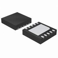
NLAS4684MNR2G ON Semiconductor, NLAS4684MNR2G Datasheet

NLAS4684MNR2G
Specifications of NLAS4684MNR2G
NLAS4684MNR2GOS
NLAS4684MNR2GOSTR
Available stocks
Related parts for NLAS4684MNR2G
NLAS4684MNR2G Summary of contents
Page 1
NLAS4684 Ultra-Low Resistance Dual SPDT Analog Switch The NLAS4684 is an advanced CMOS analog switch fabricated in Sub−micron silicon gate CMOS technology. The device is a dual Independent Single Pole Double Throw (SPDT) switch featuring of 0.5 W, for the ...
Page 2
GND 7 NC2 8 IN2 9 COM2 10 NO2 (Top View) Figure 1. Pin Connections and Logic Diagram (DFN10 and Micro10) GND B 1 NC1 IN1 COM1 3 3 ...
Page 3
MAXIMUM RATINGS Symbol V Positive DC Supply Voltage CC V Analog Input Voltage ( Digital Select Input Voltage IN I Continuous DC Current from COM to NC/NO anl1 I Peak Current from COM to NC/NO, ...
Page 4
DC ELECTRICAL CHARACTERISTICS − Analog Section Symbol Parameter R (NC) NC “ON” Resistance ON (Note 3) R (NO) NO “ON” Resistance ON (Note 3) R NC_On−Resistance FLAT (NC) Flatness (Notes NO_On−Resistance FLAT (NO) Flatness (Notes 3, 5) ...
Page 5
AC ELECTRICAL CHARACTERISTICS Symbol Parameter t Turn−On Time ON t Turn−Off Time OFF t Minimum Break−Before−Make BBM Time (Note 6) C Off NC Off Capacitance MHz NC C Off NO Off Capacitance MHz NO ...
Page 6
DUT V Output CC 0 Switch Select Pin DUT V Output CC 0.1 mF Open Input DUT Output Open Input V CC Input GND V OUT 35 pF Output GND Figure 3. t (Time Break−Before−Make) BBM V ...
Page 7
W Generator Channel switch control/s test socket is normalized. Off isolation is measured across an off channel. On loss is the bandwidth switch. V ISO V = Off Channel Isolation = 20 Log ISO V = ...
Page 8
Threshold Rising 1.2 1 Threshold Falling 0.8 0.6 0.4 0 (V) CC Figure 9. Voltage in Threshold on Logic Pins 70 60 T−on 2 T−off 2 T−off 3.0 V ...
Page 9
V 2.5 2 2.0 V 2.5 V 1.5 2 0.5 3 0.0 1.0 2.0 3.0 V (V) COM Figure 15. NC On−Resistance versus COM Voltage 0.45 +85°C 0.4 +25°C 0.35 0.3 0.25 ...
Page 10
0. 100 mA COM 0.1 0.0 1.0 2.0 V (V) COM Figure 21. NC On−Resistance versus COM Voltage 0 Bandwidth (On − Loss) ...
Page 11
... ORDERING INFORMATION Device NLAS4684FCT1 NLAS4684FCT1G NLAS4684FCTCG NLAS4684MNR2 NLAS4684MNR2G NLAS4684MR2 NLAS4684MR2G †For information on tape and reel specifications, including part orientation and tape sizes, please refer to our Tape and Reel Packaging Specifications Brochure, BRD8011/D. Package Microbump−10 Microbump−10 (Pb−Free) Microbump−10 (Pb−Free) ...
Page 12
PACKAGE DIMENSIONS 0. PIN ONE CORNER A1 0. 0.075 0. 0. Microbump−10 ...
Page 13
... Side View (Optional) 2.1746 10X 0.5651 10X 0.3008 *For additional information on our Pb−Free strategy and soldering details, please download the ON Semiconductor Soldering and Mounting Techniques Reference Manual, SOLDERRM/D. http://onsemi.com 13 NOTES: 1. DIMENSIONING AND TOLERANCING PER ASME Y14.5M, 1994. 2. CONTROLLING DIMENSION: MILLIMETERS. ...
Page 14
... SEATING H PLANE *For additional information on our Pb−Free strategy and soldering details, please download the ON Semiconductor Soldering and Mounting Techniques Reference Manual, SOLDERRM/D. ON Semiconductor and are registered trademarks of Semiconductor Components Industries, LLC (SCILLC). SCILLC reserves the right to make changes without further notice to any products herein ...


