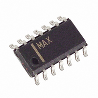
MAX4614CSD+ Maxim Integrated Products, MAX4614CSD+ Datasheet

MAX4614CSD+
Specifications of MAX4614CSD+
Related parts for MAX4614CSD+
MAX4614CSD+ Summary of contents
Page 1
... INPUT SWITCH STATE LOW OFF HIGH ON Rail-to-Rail is a registered trademark of Nippon Motorola, Ltd. ________________________________________________________________ Maxim Integrated Products For free samples & the latest literature: http://www.maxim-ic.com, or phone 1-800-998-8800. For small orders, phone 1-800-835-8769. CMOS Analog Switches ____________________________Features Fast Switching Times 12ns t ...
Page 2
Low-Voltage, High-Speed, Quad, SPST CMOS Analog Switches ABSOLUTE MAXIMUM RATINGS (Voltages referenced to GND) V ......................................................................-0.3V to +6V COM _ , NO_, NC_ (Note 1) .........................-0.3V to (V+ + 0.03V) Continuous Current (any terminal)....................................±75mA Peak Current (NO_, NC_, ...
Page 3
Low-Voltage, High-Speed, Quad, SPST ELECTRICAL CHARACTERISTICS—Single +5V Supply (continued) (V+ = +5V ±10 2.4V 0.8V, T IN_H IN_L PARAMETER SYMBOL LOGIC INPUT Input Current with Input I IN_H Voltage High Input Current with Input I IN_L ...
Page 4
Low-Voltage, High-Speed, Quad, SPST CMOS Analog Switches ELECTRICAL CHARACTERISTICS—Single +3.3V Supply (V+ = +3.3V ±10 2.4V 0.5V, T IN_H IN_L PARAMETER SYMBOL ANALOG SWITCH V COM Analog Signal Range V NO (Note On-Resistance ...
Page 5
Low-Voltage, High-Speed, Quad, SPST ELECTRICAL CHARACTERISTICS—Single +2.5V Supply (V+ = +2.5V 0. 0.5V, T INH CC INL PARAMETER SYMBOL ANALOG SWITCH V COM Analog Signal Range V NO (Note 3) V COM_ to NO_ or ...
Page 6
Low-Voltage, High-Speed, Quad, SPST CMOS Analog Switches __________________________________________Typical Operating Characteristics (V+ = +5V, GND = +25°C, unless otherwise noted.) A ON-RESISTANCE vs. V COM_ ...
Page 7
Low-Voltage, High-Speed, Quad, SPST ____________________________Typical Operating Characteristics (continued) (V+ = +5V, GND = +25°C, unless otherwise noted.) A TOTAL HARMONIC DISTORTION PLUS NOISE vs. FREQUENCY 0.050 0.045 V+ = +2V, 1Vp-p SIGNAL 0.040 0.035 0.030 V+ = ...
Page 8
Low-Voltage, High-Speed, Quad, SPST CMOS Analog Switches Applications Information Power-Supply Sequencing and Overvoltage Protection Do not exceed the absolute maximum ratings because stresses beyond the listed ratings may cause perma- nent damage to the devices. Proper power-supply sequencing is recommended ...
Page 9
Low-Voltage, High-Speed, Quad, SPST MAX4614 MAX4615 MAX4616 R GEN COM_ V GEN GND Figure 3. Charge Injection V+ 10nF SIGNAL V+ GENERATOR 0dBm COM_ ANALYZER NO_, NC_ GND R L Figure 4. Off-Isolation/On-Channel Bandwidth _______________________________________________________________________________________ CMOS Analog Switches Test Circuits/Timing ...
Page 10
Low-Voltage, High-Speed, Quad, SPST CMOS Analog Switches Test Circuits/Timing Diagrams V+ 10nF V+ COM_ CAPACITANCE METER NO_, NC_ f = 1MHz GND Figure 6. Channel Off/On-Capacitance 10 ______________________________________________________________________________________ Ordering Information (continued) (continued) PART MAX4615CUD MAX4615CSD MAX4615CPD MAX4615EUD MAX4614 MAX4615ESD MAX4615 ...
Page 11
Low-Voltage, High-Speed, Quad, SPST ______________________________________________________________________________________ CMOS Analog Switches Package Information 11 ...
Page 12
... Maxim cannot assume responsibility for use of any circuitry other than circuitry entirely embodied in a Maxim product. No circuit patent licenses are implied. Maxim reserves the right to change the circuitry and specifications without notice at any time. 12 ____________________Maxim Integrated Products, 120 San Gabriel Drive, Sunnyvale, CA 94086 408-737-7600 © 1999 Maxim Integrated Products ...


