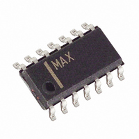
MAX4614CSD+ Maxim Integrated Products, MAX4614CSD+ Datasheet - Page 8

MAX4614CSD+
Manufacturer Part Number
MAX4614CSD+
Description
IC SWITCH QUAD SPST 14SOL
Manufacturer
Maxim Integrated Products
Datasheet
1.MAX4614CSD.pdf
(12 pages)
Specifications of MAX4614CSD+
Function
Switch
Circuit
4 x SPST - NO
On-state Resistance
10 Ohm
Voltage Supply Source
Single Supply
Voltage - Supply, Single/dual (±)
2 V ~ 5.5 V
Current - Supply
1µA
Operating Temperature
0°C ~ 70°C
Mounting Type
Surface Mount
Package / Case
14-SOIC (0.154", 3.90mm Width)
Number Of Switches
Quad
Switch Configuration
SPST
On Resistance (max)
10 Ohms
On Time (max)
12 ns
Off Time (max)
10 ns
Off Isolation (typ)
- 85 dB
Supply Voltage (max)
5.5 V
Supply Voltage (min)
2 V
Supply Current
0.001 uA
Maximum Power Dissipation
640 mW
Maximum Operating Temperature
+ 70 C
Mounting Style
SMD/SMT
Description/function
Analog Switch
Input Level
CMOS, TTL
Minimum Operating Temperature
0 C
Off State Leakage Current (max)
1 nA
Lead Free Status / RoHS Status
Lead free / RoHS Compliant
Do not exceed the absolute maximum ratings because
stresses beyond the listed ratings may cause perma-
nent damage to the devices.
Proper power-supply sequencing is recommended for
all CMOS devices. Always apply V+ before applying
analog signals or logic inputs, especially if the analog
or logic signals are not current limited. If this sequenc-
ing is not possible, and if the analog or logic inputs are
not current limited to 20mA, add a small-signal diode
(D1) as shown in Figure 1. If the analog signal can dip
below GND, add D2. Adding protection diodes
reduces the analog signal range to a diode drop (about
0.7V) below V+ (for D1), and to a diode drop above
ground (for D2). Leakage is unaffected by adding the
diodes. On-resistance increases by a small amount at
low supply voltages. Maximum supply voltage (V+)
must not exceed 6V.
Adding protection diodes causes the logic thresholds
to be shifted relative to the power-supply rails. This can
be significant when low supply voltages (+5V or less)
are used. With a +5V supply, TTL compatibility is not
guaranteed when protection diodes are added. Driving
IN1 and IN2 all the way to the supply rails (i.e., to a
Low-Voltage, High-Speed, Quad, SPST
CMOS Analog Switches
Figure 2. Switching Time
8
______________________________________________Test Circuits/Timing Diagrams
_______________________________________________________________________________________
MAX4614
MAX4615
MAX4616
SWITCH
INPUT
LOGIC
INPUT
V
COM
Applications Information
Power-Supply Sequencing and
_
C
V
OUT
L
INCLUDES FIXTURE AND STRAY CAPACITANCE.
COM_
IN_
= V
GND
COM
Overvoltage Protection
(
R
L
R
+ R
L
V+
V+
ON
)
NO_, NC_
R
300
L
SWITCH
OUTPUT
C
35pF
L
V
OUT
diode drop higher than the V+ pin, or to a diode drop
lower than the GND pin) is always acceptable.
Protection diodes D1 and D2 also protect against some
overvoltage situations. With Figure 1’s circuit, if the sup-
ply voltage is below the absolute maximum rating, and
if a fault voltage up to the absolute maximum rating is
applied to an analog signal pin, no damage will result.
Figure 1. Overvoltage Protection Using Two External Blocking
Diodes
OUTPUT
SWITCH
LOGIC
INPUT
V g
V
INH
0
0
NO_
V
OUT
t
ON
50%
POSITIVE SUPPLY
0.9
·
V+
V
D2
0UT
D1
COM_
t
OFF
50%
t
t
MAX4614
MAX4615
MAX4616
R
F
0.9
< 20ns
< 20ns
·
V
OUT


