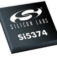
SI5374B-A-GL Silicon Laboratories Inc, SI5374B-A-GL Datasheet - Page 14

SI5374B-A-GL
Manufacturer Part Number
SI5374B-A-GL
Description
Clock Synthesizer / Jitter Cleaner QUAD DSPLL JITT ATT CLK LO LP BW 8IN/OUT
Manufacturer
Silicon Laboratories Inc
Datasheet
1.SI5374B-A-GL.pdf
(64 pages)
Specifications of SI5374B-A-GL
Package / Case
PBGA-80
Input Level
LVCMOS
Max Input Freq
525 Hz
Max Output Freq
808 MHz
Maximum Operating Temperature
+ 85 C
Minimum Operating Temperature
- 40 C
Number Of Outputs
8
Output Level
LVCMOS
Supply Current
1100 mA
Supply Voltage (max)
2.8 V
Supply Voltage (min)
- 0.5 V
Lead Free Status / Rohs Status
Compliant
Available stocks
Company
Part Number
Manufacturer
Quantity
Price
Company:
Part Number:
SI5374B-A-GL
Manufacturer:
SILICON
Quantity:
1 001
Company:
Part Number:
SI5374B-A-GL
Manufacturer:
Silicon Laboratories Inc
Quantity:
10 000
Si5374
3. Functional Description
The Si5374 is a highly integrated jitter-attenuating clock multiplier that integrates four fully independent DSPLLs
and provides ultra-low jitter generation with less than 400 fs RMS. Configuration and control of the Si5374 is mainly
handled through the I
independent, synchronous clock outputs ranging from 2 kHz to 808 MHz for each DSPLL. Virtually any frequency
translation (M/N) combination across its operating range is supported. The Si5374 supports a digitally
programmable loop bandwidth that can range from 4 to 525 Hz requiring no external DSPLL components. An
external single-ended or differential reference clock or XO is required for the device to enable ultra-low jitter
generation and jitter attenuation.
The device monitors each input clock for loss-of-signal (LOS) and provides a LOS alarm when missing pulses on
any of the input clocks are detected. The device monitors the lock status of each DSPLL and provides a Loss-of-
Lock (LOL) alarm when the DSPLL is unlocked. The lock detect algorithm continuously monitors the phase of the
selected input clock in relation to the phase of the feedback clock. The Si5374 provides a holdover capability that
allows the device to continue generation of a stable output clock when the input reference is lost. The reference
oscillator can be internally routed into CKIN2_q, so free-running clock generation is supported for each DSPLL
offering simultaneous synchronous and asynchronous operation.
The output drivers are configurable to support common signal formats, such as LVPECL, LVDS, CML, and CMOS
loads. If the CMOS signal format is selected, each differential output buffer generates two in-phase CMOS clocks
at the same frequency. For system-level debugging, a DSPLL bypass mode drives the clock output directly from
the selected input clock, bypassing the internal DSPLL.
Silicon Laboratories offers a PC-based software utility, DSPLLsim that can be used to determine valid frequency
plans and loop bandwidth settings to simplify device setup. DSPLLsim provides the optimum input, output, and
feedback divider values for a given input frequency and clock multiplication ratio that minimizes phase noise. This
utility can be downloaded from http://www.silabs.com/timing. For further assistance, refer to the Si53xx Any-
14
2
C interface. The device accepts clock inputs ranging from 2 kHz to 710 MHz and generates
CKIN1N_A
CKIN2N_A
CKIN3N_B
CKIN4N_B
CKIN5N_C
CKIN6N_C
CKIN7N_D
CKIN8N_D
CKIN1P_A
CKIN2P_A
CKIN3P_B
CKIN4P_B
CKIN5P_C
CKIN6P_C
CKIN7P_D
CKIN8P_D
CS_CA_q
RSTL_q
Internal
Internal
Internal
Internal
Osc
Osc
Osc
Osc
SCL
SDA LOL_q IRQ_q
Figure 3. Functional Block Diagram
Input Stage
Status / Control
÷ N31
÷ N32
÷ N31
÷ N32
÷ N31
÷ N32
÷ N31
÷ N32
Monitor
Monitor
Monitor
Monitor
Hitless
Switch
Hitless
Switch
Hitless
Switch
Hitless
Switch
PLL Bypass
PLL Bypass
PLL Bypass
PLL Bypass
Input
Input
Input
Input
OSC_P/N
Preliminary Rev. 0.4
XO or Clock
Low Jitter
f
f
f
f
3
3
3
3
DSPLL
DSPLL
DSPLL
DSPLL
Synthesis Stage
A
÷ N2
B
÷ N2
C
÷ N2
D
÷ N2
®
®
®
®
f
f
f
f
OSC
OSC
OSC
OSC
÷
÷
÷
÷
NC1_HS
NC1_HS
NC1_HS
NC1_HS
PLL Bypass
PLL Bypass
PLL Bypass
PLL Bypass
PLL Bypass
PLL Bypass
PLL Bypass
PLL Bypass
÷ NC1
÷ NC1
÷ NC1
÷ NC1
÷ NC2
÷ NC2
÷ NC2
÷ NC2
Voltage Regulator
Output Stage
High PSRR
CKOUT2P_A
CKOUT2N_A
CKOUT4P_B
CKOUT4N_B
CKOUT6P_C
CKOUT6N_C
CKOUT8P_D
CKOUT8N_D
CKOUT1P_A
CKOUT1N_A
CKOUT3P_B
CKOUT3N_B
CKOUT5P_C
CKOUT5N_C
CKOUT7P_D
CKOUT7N_D
VDD_q
GND


