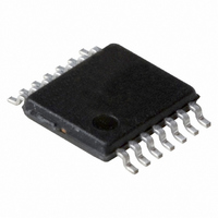
74LVC4066PW,118 NXP Semiconductors, 74LVC4066PW,118 Datasheet - Page 4

74LVC4066PW,118
Manufacturer Part Number
74LVC4066PW,118
Description
IC SWITCH QUAD SPST 14TSSOP
Manufacturer
NXP Semiconductors
Series
74LVCr
Type
Analog Switchr
Datasheet
1.74LVC4066BQ115.pdf
(23 pages)
Specifications of 74LVC4066PW,118
Package / Case
14-TSSOP (0.173", 4.40mm Width)
Function
Switch
Circuit
4 x SPST - NO
On-state Resistance
6 Ohm
Voltage Supply Source
Single Supply
Voltage - Supply, Single/dual (±)
1.65 V ~ 5.5 V
Current - Supply
0.1µA
Operating Temperature
-40°C ~ 125°C
Mounting Type
Surface Mount
Switch Configuration
SPST
On Resistance (max)
34 Ohm (Typ) @ 1.95 V
On Time (max)
5.3 ns (Typ) @ 1.95 V
Off Time (max)
4.2 ns (Typ) @ 1.95 V
Supply Voltage (max)
5.5 V
Supply Voltage (min)
1.65 V
Maximum Power Dissipation
500 mW
Maximum Operating Temperature
+ 125 C
Mounting Style
SMD/SMT
Minimum Operating Temperature
- 40 C
Package
14TSSOP
Maximum On Resistance
195@1.95V Ohm
Maximum Propagation Delay Bus To Bus
0.2(Typ)@5.5V|0.3(Typ)@3.6V|0.4(Typ)@2.7V|0.8(Typ)@1.95V ns
Maximum Low Level Output Current
50 mA
Maximum Turn-off Time
4.2(Typ)@1.95V ns
Maximum Turn-on Time
5.3(Typ)@1.95V ns
Switch Architecture
SPST
Power Supply Type
Single
Lead Free Status / RoHS Status
Lead free / RoHS Compliant
Lead Free Status / RoHS Status
Lead free / RoHS Compliant, Lead free / RoHS Compliant
Other names
74LVC4066PW-T
74LVC4066PW-T
935273718118
74LVC4066PW-T
935273718118
NXP Semiconductors
6. Functional description
Table 3.
[1]
7. Limiting values
Table 4.
In accordance with the Absolute Maximum Rating System (IEC 60134). Voltages are referenced to GND (ground = 0 V).
[1]
[2]
[3]
74LVC4066
Product data sheet
Input nE
L
H
Symbol
V
V
I
I
V
I
I
I
T
P
IK
SK
SW
CC
GND
stg
CC
I
SW
tot
H = HIGH voltage level;
L = LOW voltage level.
The minimum input voltage rating may be exceeded if the input current rating is observed.
The minimum and maximum switch voltage ratings may be exceeded if the switch clamping current rating is observed.
For SO14 packages: above 70 C derate linearly with 8 mW/K.
For (T)SSOP14 packages: above 60 C derate linearly with 5.5 mW/K.
For DHVQFN14 packages: above 60 C derate linearly with 4.5 mW/K.
Function table
Limiting values
Parameter
supply voltage
input voltage
input clamping current
switch clamping current
switch voltage
switch current
supply current
ground current
storage temperature
total power dissipation
[1]
All information provided in this document is subject to legal disclaimers.
Conditions
V
V
enable and disable mode
0.5 < V
T
amb
I
I
< 0.5 V or V
< 0.5 V or V
Rev. 4 — 24 November 2010
= 40 C to +125 C
SW
< V
CC
I
I
Switch
OFF
ON
< V
< V
+ 0.5 V
CC
CC
+ 0.5 V
+ 0.5 V
[1]
[2]
[3]
Min
0.5
0.5
50
-
0.5
-
-
100
65
-
74LVC4066
Max
+6.5
+6.5
-
50
+6.5
50
100
-
+150
500
Quad bilateral switch
© NXP B.V. 2010. All rights reserved.
Unit
V
V
mA
mA
V
mA
mA
mA
C
mW
4 of 23


