MMPQ3904R1 ON Semiconductor, MMPQ3904R1 Datasheet
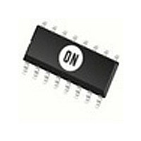
MMPQ3904R1

Manufacturer Part Number
MMPQ3904R1
Description
Manufacturer
ON Semiconductor
Datasheet

Specifications of MMPQ3904R1

Transistor Polarity
NPN
Number Of Elements
4
Collector-emitter Voltage
40V
Collector-base Voltage
60V
Emitter-base Voltage
6V
Collector Current (dc) (max)
200mA
Dc Current Gain (min)
30
Power Dissipation
800mW
Frequency (max)
300MHz
Operating Temp Range
-55C to 150C
Operating Temperature Classification
Military
Mounting
Surface Mount
Pin Count
16
Package Type
SOIC
Lead Free Status / Rohs Status
Not Compliant
NPN Silicon
Preferred devices are ON Semiconductor recommended choices for future use and best overall value.
1. Pulse Test: Pulse Width v 300 ms; Duty Cycle v 2.0%.
March, 2001 – Rev. 2
MAXIMUM RATINGS
ELECTRICAL CHARACTERISTICS
OFF CHARACTERISTICS
Collector–Emitter Voltage
Collector–Base Voltage
Emitter–Base Voltage
Collector Current — Continuous
Total Power Dissipation
Operating and Storage
Collector–Emitter Breakdown Voltage (1)
Collector–Base Breakdown Voltage
Emitter–Base Breakdown Voltage
Collector Cutoff Current
Emitter Cutoff Current
Semiconductor Components Industries, LLC, 2001
@ T A = 25 C
Derate above 25 C
@ T C = 25 C
Derate above 25 C
Junction Temperature Range
(I C = 1.0 mAdc, I B = 0)
(I C = 10 mAdc, I E = 0)
(I E = 10 mAdc, I C = 0)
(V CB = 40 Vdc, I E = 0)
(V EB = 4.0 Vdc, I C = 0)
Rating
Characteristic
t
Symbol
T J , T stg
V CEO
(T A = 25 C unless otherwise noted)
V CB
V EB
P D
P D
I C
V (BR)CEO
V (BR)CBO
V (BR)EBO
Symbol
I CBO
I EBO
Transistor
Each
0.66
0.4
3.2
5.3
–55 to +150
Min
6.0
40
60
Value
200
6.0
40
60
1
Equal Power
Transistors
Typ
Four
1.92
15.4
800
6.4
Max
50
50
mW/ C
mW/ C
mAdc
Watts
Unit
Vdc
Vdc
Vdc
mW
nAdc
nAdc
Unit
Vdc
Vdc
Vdc
C
ON Semiconductor Preferred Device
CASE 751B–05, STYLE 4
16
Publication Order Number:
SO–16
1
MMPQ3904/D

Related parts for MMPQ3904R1

MMPQ3904R1 Summary of contents

Page 1

... Collector Cutoff Current ( Vdc Emitter Cutoff Current ( 4.0 Vdc Pulse Test: Pulse Width v 300 ms; Duty Cycle v 2.0%. Preferred devices are ON Semiconductor recommended choices for future use and best overall value. Semiconductor Components Industries, LLC, 2001 March, 2001 – Rev. 2 Symbol Value ...

Page 2

ELECTRICAL CHARACTERISTICS Characteristic ON CHARACTERISTICS (1) DC Current Gain ( 0.1 mAdc 1.0 Vdc 1.0 mAdc 1.0 Vdc mAdc 1.0 Vdc) Collector–Emitter ...

Page 3

INFORMATION FOR USING THE SO–16 SURFACE MOUNT PACKAGE MINIMUM RECOMMENDED FOOTPRINT FOR SURFACE MOUNTED APPLICATIONS Surface mount board layout is a critical portion of the total design. The footprint for the semiconductor packages must be the correct size to insure ...

Page 4

... SO–16 ISSUE J –B– JAPAN: ON Semiconductor, Japan Customer Focus Center 4–32–1 Nishi–Gotanda, Shinagawa–ku, Tokyo, Japan 141–0031 Phone: 81–3–5740–2700 Email: r14525@onsemi.com ON Semiconductor Website: http://onsemi.com For additional information, please contact your local Sales Representative. http://onsemi.com ...

Related keywords