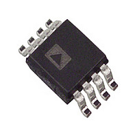
ADG918BRM-500RL7 Analog Devices Inc, ADG918BRM-500RL7 Datasheet - Page 6

ADG918BRM-500RL7
Manufacturer Part Number
ADG918BRM-500RL7
Description
Manufacturer
Analog Devices Inc
Datasheet
1.ADG918BRM-500RL7.pdf
(16 pages)
Specifications of ADG918BRM-500RL7
Frequency (max)
2GHz
Insertion Loss (max)
1.25dB
Pin Count
8
Package Type
MSOP
Lead Free Status / Rohs Status
Not Compliant
ADG918/ADG919
PIN CONFIGURATION AND FUNCTION DESCRIPTIONS
Table 3. Pin Function Descriptions
Pin No.
1
2
3, 6, 7
4
5
8
Table 4. Truth Table
CTRL
0
1
Mnemonic
V
CTRL
GND
RFC
RF2
RF1
DD
Signal Path
RF2 to RFC
RF1 to RFC
Function
Power Supply Input. These parts can be operated from 1.65 V to 2.75 V, and V
Logic Control Input. See Table 4.
Ground Reference Point for All Circuitry on the Part.
COMMON RF Port for Switch.
RF2 Port.
RF1 Port.
Exposed Pad Tied to Substrate, GND
8-Lead 3 mm x 3 mm LFCSP (CP-8);
Figure 4. 8-Lead MSOP (RM-8) and
CTRL
GND
RFC
V
DD
Rev. C | Page 6 of 16
1
2
3
4
(Not to Scale)
ADG918/
ADG919
TOP VIEW
8
7
6
5
RF1
GND
GND
RF2
DD
should be decoupled to GND.


