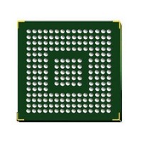
STM32F407IGH6 STMicroelectronics, STM32F407IGH6 Datasheet - Page 25

STM32F407IGH6
Manufacturer Part Number
STM32F407IGH6
Description
Microcontrollers (MCU) ARM M4 1024 FLASH 168 Mhz 192kB SRAM
Manufacturer
STMicroelectronics
Datasheet
1.STM32F407ZGT6.pdf
(167 pages)
Specifications of STM32F407IGH6
Core
ARM Cortex M4
Processor Series
STM32F4
Data Bus Width
32 bit
Maximum Clock Frequency
168 MHz
Program Memory Size
1024 KB
Data Ram Size
192 KB
On-chip Adc
Yes
Number Of Programmable I/os
140
Number Of Timers
10
Operating Supply Voltage
1.7 V to 3.6 V
Package / Case
UFBGA-176
Mounting Style
SMD/SMT
A/d Bit Size
12 bit
A/d Channels Available
24
Interface Type
CAN, I2C, I2S, SPI, UART
Program Memory Type
Flash
Lead Free Status / Rohs Status
Details
Available stocks
Company
Part Number
Manufacturer
Quantity
Price
Company:
Part Number:
STM32F407IGH6
Manufacturer:
STMicroelectronics
Quantity:
1
Company:
Part Number:
STM32F407IGH6
Manufacturer:
STMicroelectronics
Quantity:
10 000
Part Number:
STM32F407IGH6
Manufacturer:
ST
Quantity:
20 000
STM32F405xx, STM32F407xx
Regulator OFF
This mode allows to power the device as soon as V
●
●
Regulator OFF/internal reset ON
This mode is available only on UFBGA package. It is activated by setting
BYPASS_REG and PDR_ON pins to V
The regulator OFF/internal reset ON mode allows to supply externally a 1.2 V voltage
source through V
The following conditions must be respected:
–
–
–
In regulator OFF/internal reset ON mode, PA0 cannot be used as a GPIO pin since it
allows to reset the part of the 1.2 V logic which is not reset by the NRST pin, when the
internal voltage regulator in off.
Regulator OFF/internal reset OFF
This mode is available only on UFBGA package. It is activated by setting
BYPASS_REG pin to V
allows to supply externally a 1.2 V voltage source through V
addition to V
The following conditions must be respected:
–
–
–
V
between power domains.
If the time for V
reach 1.8 V (V
operates in the 0 to 70 °C temperature range and PDR is disabled), then PA0
should be connected to the NRST pin (see
asserted low externally during POR until V
If V
must be asserted on PA0 pin.
V
between power domains.
PA0 should be kept low to cover both conditions: until V
1.08 V and until V
NRST should be controlled by an external reset controller to keep the device
under reset when V
DD
DD
CAP_1
should always be higher than V
should always be higher than V
DD
and V
.
CAP_1
DD
CAP_1
CAP_2
/V
DD
and V
DD
DDA
DD
Doc ID 022152 Rev 2
reaches 1.8 V (see
and V
and by applying an inverted reset signal to PDR_ON, and
go below 1.08 V and V
is below 1.8 V (see
minimum value of 1.7 V is obtained when the device
CAP_2
CAP_2
pins, in addition to V
to reach 1.08 V is faster than the time for V
DD
CAP_1
CAP_1
.
Figure
DD
and V
DD
and V
Figure
Figure
DD
reaches 1.8 V.
reaches 1.8 V (see
8).
is higher than 1.7 V, then a reset
CAP_2
CAP_2
9).
8). Otherwise, PA0 should be
DD
.
to avoid current injection
to avoid current injection
CAP_1
CAP_1
and V
and V
Figure
CAP_2
CAP_2
Description
9).
pins, in
reach
25/167
DD
to


