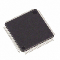
DS21354LN Maxim Integrated Products, DS21354LN Datasheet - Page 39

DS21354LN
Manufacturer Part Number
DS21354LN
Description
IC TXRX E1 1-CHIP 3.3V 100-LQFP
Manufacturer
Maxim Integrated Products
Datasheet
1.DS2154LNA2.pdf
(124 pages)
Specifications of DS21354LN
Function
Single-Chip Transceiver
Interface
E1, HDLC
Number Of Circuits
1
Voltage - Supply
3.14 V ~ 3.47 V
Current - Supply
75mA
Operating Temperature
-40°C ~ 85°C
Mounting Type
Surface Mount
Package / Case
100-LQFP
Includes
Remote and AIS Alarm Detector / Generator
Lead Free Status / RoHS Status
Contains lead / RoHS non-compliant
Power (watts)
-
Available stocks
Company
Part Number
Manufacturer
Quantity
Price
Company:
Part Number:
DS21354LN+
Manufacturer:
Maxim
Quantity:
180
Company:
Part Number:
DS21354LN+
Manufacturer:
DALLAS
Quantity:
1 085
CCR3: COMMON CONTROL REGISTER 3 (Address=1B Hex)
SYMBOL
(MSB)
TESE
TCBFS
TIRFS
RCLA
RSRE
THSE
TBCS
TESE
-
TCBFS
POSITION
CCR3.7
CCR3.6
CCR3.5
CCR3.4
CCR3.3
CCR3.2
CCR3.1
CCR3.0
TIRFS
Transmit-Side Elastic Store Enable.
0 = elastic store is bypassed
1 = elastic store is enabled
Transmit Channel Blocking Registers (TCBR) Function Select.
0 = TCBRs define the operation of the TCHBLK output pin
1 = TCBRs define which signaling bits are to be inserted
Transmit Idle Registers (TIR) Function Select. See Section
details.
0 = TIRs define in which channels to insert idle code
1 = TIRs define in which channels to insert data from RSER (i.e., Per-
Cannel Loopback function)
Not Assigned. Should be set to zero when written to.
Receive-Side Signaling Reinsertion Enable. See Section
0 = do not reinsert signaling bits into the data stream presented at the
RSER pin
1 = reinsert the signaling bits into data stream presented at the RSER pin
Transmit-Side Hardware Signaling Insertion Enable. See Section
for details.
0 = do not insert signaling from the TSIG pin into the data stream
presented at the TSER pin
1 = insert signaling from the TSIG pin into the data stream presented at
the TSER pin
Transmit-Side Backplane Clock Select.
0 = if TSYSCLK is 1.544MHz
1 = if TSYSCLK is 2.048MHz/4.096MHz/8.192MHz
Receive Carrier Loss (RCL) Alternate Criteria.
0 = RCL declared upon 255 consecutive zeros (125ms)
1 = RCL declared upon 2048 consecutive zeros (1ms)
—
39 of 124
NAME AND DESCRIPTION
RSRE
THSE
TBCS
10.2
10.1
for details.
RCLA
(LSB)
for
10.1


