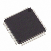
DS21354LN Maxim Integrated Products, DS21354LN Datasheet - Page 79

DS21354LN
Manufacturer Part Number
DS21354LN
Description
IC TXRX E1 1-CHIP 3.3V 100-LQFP
Manufacturer
Maxim Integrated Products
Datasheet
1.DS2154LNA2.pdf
(124 pages)
Specifications of DS21354LN
Function
Single-Chip Transceiver
Interface
E1, HDLC
Number Of Circuits
1
Voltage - Supply
3.14 V ~ 3.47 V
Current - Supply
75mA
Operating Temperature
-40°C ~ 85°C
Mounting Type
Surface Mount
Package / Case
100-LQFP
Includes
Remote and AIS Alarm Detector / Generator
Lead Free Status / RoHS Status
Contains lead / RoHS non-compliant
Power (watts)
-
Available stocks
Company
Part Number
Manufacturer
Quantity
Price
Company:
Part Number:
DS21354LN+
Manufacturer:
Maxim
Quantity:
180
Company:
Part Number:
DS21354LN+
Manufacturer:
DALLAS
Quantity:
1 085
TDC1: TRANSMIT HDLC DS0 CONTROL REGISTER 1 (Address = BA Hex)
TDC2: TRANSMIT HDLC DS0 CONTROL REGISTER 2 (Address = BB Hex)
SYMBOL
SYMBOL
(MSB)
(MSB)
TDS0M
TDB8
TSaDS
THE
TDB8
TDB7
TDB6
TDB5
TDB4
TDB3
TDB2
TDB1
THE
TD4
TD3
TD2
TD1
TD0
TSaDS
POSITION
POSITION
TDB7
TDC1.7
TDC1.6
TDC1.5
TDC1.4
TDC1.3
TDC1.2
TDC1.1
TDC1.0
TDC2.7
TDC2.6
TDC2.5
TDC2.4
TDC2.3
TDC2.2
TDC2.1
TDC2.0
TDS0M
TDB6
Transmit HDLC Enable.
0 = disable HDLC controller (no data inserted by HDLC controller into
the transmit data stream)
1 = enable HDLC controller to allow insertion of HDLC data into either
the Sa position or multiple DS0 channels as defined by TDC1 (see bit
definitions below).
Transmit Sa Bit / DS0 Select. This bit is ignored if TDC1.7 is set to zero.
0 = route Sa bits from the HDLC controller. TD0 to TD4 defines which Sa
bits are to be routed. TD4 corresponds to Sa4, TD3 to Sa5, TD2 to Sa6,
TD1 to Sa7 and TD0 to Sa8.
1 = route DS0 channels from the HDLC controller. TDC1.5 is used to
determine how the DS0 channels are selected.
DS0 Selection Mode.
0 = utilize the TD0 to TD4 bits to select which single DS0 channel to use.
1 = utilize the TCHBLK control registers to select which DS0 channels to
use.
DS0 Channel Select Bit 4. MSB of the DS0 channel select.
DS0 Channel Select Bit 3.
DS0 Channel Select Bit 2.
DS0 Channel Select Bit 1.
DS0 Channel Select Bit 0. LSB of the DS0 channel select.
DS0 Bit 8 Suppress Enable. MSB of the DS0. Set to one to stop this bit
from being used.
DS0 Bit 7 Suppress Enable. Set to one to stop this bit from being used.
DS0 Bit 6 Suppress Enable. Set to one to stop this bit from being used.
DS0 Bit 5 Suppress Enable. Set to one to stop this bit from being used.
DS0 Bit 4 Suppress Enable. Set to one to stop this bit from being used.
DS0 Bit 3 Suppress Enable. Set to one to stop this bit from being used.
DS0 Bit 2 Suppress Enable. Set to one to stop this bit from being used.
DS0 Bit 1 Suppress Enable. LSB of the DS0. Set to one to stop this bit
from being used.
TDB5
TD4
79 of 124
NAME AND DESCRIPTION
NAME AND DESCRIPTION
TDB4
TD3
TDB3
TD2
TDB2
TD1
(LSB)
(LSB)
TDB1
TD0


