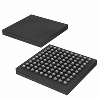
DS3170N+ Maxim Integrated Products, DS3170N+ Datasheet - Page 66

DS3170N+
Manufacturer Part Number
DS3170N+
Description
IC TXRX DS3/E3 100-CSBGA
Manufacturer
Maxim Integrated Products
Datasheet
1.DS3170.pdf
(230 pages)
Specifications of DS3170N+
Function
Single-Chip Transceiver
Interface
DS3, E3
Number Of Circuits
1
Voltage - Supply
3.135 V ~ 3.465 V
Current - Supply
120mA
Operating Temperature
-40°C ~ 85°C
Mounting Type
Surface Mount
Package / Case
100-LBGA
Includes
DS3 Framers, E3 Framers, HDLC Controller, On-Chip BERTs
Lead Free Status / RoHS Status
Lead free / RoHS Compliant
Power (watts)
-
- Current page: 66 of 230
- Download datasheet (3Mb)
10.4 Global Resources
10.4.1 Clock Rate Adapter (CLAD)
The clock rate adapter is composed of a PLL block to create the internal clock which can be used for the transmit
clock and/or LIU reference clock from a clock input on the reference input (REFCLK) pin. The device needs one of
two (DS3 or E3) internal clock rates. The input reference clock frequency can be either 44.736, 34.368. 77.78,
51.84 or 19.44 MHz.
The receive LIU is supplied a reference clock from the CLAD. The receive LIU selects the clock frequency based
upon the mode the user selects via the FM bits. The CLAD output is also available as a transmit clock source if
selected via the PORT.CR2.CLADC register bit.
The user must supply at least one of the five rates (44.736, 34.368. 77.78, 51.84 or 19.4 MHz) to the REFCLK pin.
The CLAD[2:0] bits informs the PLL of the frequency applied to the pins. Selection of the clock applied to the LIU
and optionally the transmitter is controlled by the FM bits (located in PORT.CR2). The CLAD allows maximum
flexibility to the user. The user may supply any of the five clock rates and use the CLAD to convert the rate to the
particular clock rate needed for his application.
The CLAD PLL is enabled when the CLAD input reference clock is different from the clock required for the framing
mode. The CLAD PLL is disabled and the CLAD output clock is connected directly to the CLAD input clock
(REFCLK) when the framing mode requires the same clock as the CLAD input reference clock.
Table 10-11. CLAD Clock Source Settings
10.4.2 8 kHz Reference Generation
The global 8KREF signal is used to generate the one second reference signal by dividing it by 8000. This signal
can be derived from almost any clock source on the chip as well as the general purpose IO pin GPIO4. The port
8KREF signal can be sourced from the transmit or receive clocks. The minimum input frequency stability of the
8KREF input pin is +/- 500 ppm.
The global 8KREF signal can come from an external 8000 Hz reference connected to the GPIO4 general purpose
IO pin by setting the GL.CR2.G8KIS bit. The global 8KREF signal can be output on the GPIO2 general purpose IO
pin when the GL.CR2.G8KOS bit is set.
The global 8KREF signal can be derived from the CLAD PLL or pins or come from any of the port 8KREF signals
by clearing GL.CR2.G8KIS bit and selecting the source using the
The port 8KREF signal can be derived from the transmit clock input pin or from the receive LIU or input clock pin.
The
The 8KREF 8.000 kHz signal is a simple divisor of 44736 kHz (DS3 divided by 5592) or 33368 kHz (E3 divided by
4296). The correct divisor for the port 8KREF source is selected by the mode the port is configured for. The CLAD
clock chosen for the clock source selects the correct divisor for the global 8KREF. The 8KREF signal is only as
accurate as the clock source chosen to generate it.
Table 10-12
CLAD[2:0]
PORT.CR3.
11X
000
001
010
011
100
101
lists the selectable sources for global 8 kHz reference.
P8KRS[1:0] bits are used to select which source.
REFCLK (INPUT)
44.736 MHz
34.368 MHz
51.84 MHz
19.44 MHz
Undefined
Undefined
77.76 MHz
66 of 230
GL.CR2.
DS3170 DS3/E3 Single-Chip Transceiver
G8KRS[2:0] bits.
Related parts for DS3170N+
Image
Part Number
Description
Manufacturer
Datasheet
Request
R

Part Number:
Description:
IC TXRX DS3/E3 100-CSBGA
Manufacturer:
Maxim Integrated Products
Datasheet:

Part Number:
Description:
Network Controller & Processor ICs DS3-E3 Single-Chip T ransceiver T3-E3 Fra
Manufacturer:
Maxim Integrated Products
Datasheet:

Part Number:
Description:
MAX7528KCWPMaxim Integrated Products [CMOS Dual 8-Bit Buffered Multiplying DACs]
Manufacturer:
Maxim Integrated Products
Datasheet:

Part Number:
Description:
Single +5V, fully integrated, 1.25Gbps laser diode driver.
Manufacturer:
Maxim Integrated Products
Datasheet:

Part Number:
Description:
Single +5V, fully integrated, 155Mbps laser diode driver.
Manufacturer:
Maxim Integrated Products
Datasheet:

Part Number:
Description:
VRD11/VRD10, K8 Rev F 2/3/4-Phase PWM Controllers with Integrated Dual MOSFET Drivers
Manufacturer:
Maxim Integrated Products
Datasheet:

Part Number:
Description:
Highly Integrated Level 2 SMBus Battery Chargers
Manufacturer:
Maxim Integrated Products
Datasheet:

Part Number:
Description:
Current Monitor and Accumulator with Integrated Sense Resistor; ; Temperature Range: -40°C to +85°C
Manufacturer:
Maxim Integrated Products

Part Number:
Description:
TSSOP 14/A°/RS-485 Transceivers with Integrated 100O/120O Termination Resis
Manufacturer:
Maxim Integrated Products

Part Number:
Description:
TSSOP 14/A°/RS-485 Transceivers with Integrated 100O/120O Termination Resis
Manufacturer:
Maxim Integrated Products

Part Number:
Description:
QFN 16/A°/AC-DC and DC-DC Peak-Current-Mode Converters with Integrated Step
Manufacturer:
Maxim Integrated Products

Part Number:
Description:
TDFN/A/65V, 1A, 600KHZ, SYNCHRONOUS STEP-DOWN REGULATOR WITH INTEGRATED SWI
Manufacturer:
Maxim Integrated Products

Part Number:
Description:
Integrated Temperature Controller f
Manufacturer:
Maxim Integrated Products

Part Number:
Description:
SOT23-6/I°/45MHz to 650MHz, Integrated IF VCOs with Differential Output
Manufacturer:
Maxim Integrated Products

Part Number:
Description:
SOT23-6/I°/45MHz to 650MHz, Integrated IF VCOs with Differential Output
Manufacturer:
Maxim Integrated Products


