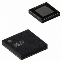
SC16C752BIBS,151 NXP Semiconductors, SC16C752BIBS,151 Datasheet - Page 17

SC16C752BIBS,151
Manufacturer Part Number
SC16C752BIBS,151
Description
IC UART DUAL W/FIFO 32-HVQFN
Manufacturer
NXP Semiconductors
Type
Dual UART with 64-byte FIFOsr
Datasheet
1.SC16C752BIBS151.pdf
(47 pages)
Specifications of SC16C752BIBS,151
Number Of Channels
2, DUART
Package / Case
32-VFQFN Exposed Pad
Features
False-start Bit Detection
Fifo's
64 Byte
Voltage - Supply
2.5V, 3.3V, 5V
With Auto Flow Control
Yes
With False Start Bit Detection
Yes
With Modem Control
Yes
Mounting Type
Surface Mount
Data Rate
5 Mbps
Supply Voltage (max)
5.5 V
Supply Voltage (min)
2.25 V
Supply Current
4.5 mA
Maximum Operating Temperature
+ 85 C
Minimum Operating Temperature
- 40 C
Mounting Style
SMD/SMT
Operating Supply Voltage
2.5 V or 3.3 V or 5 V
Lead Free Status / RoHS Status
Lead free / RoHS Compliant
Lead Free Status / RoHS Status
Lead free / RoHS Compliant, Lead free / RoHS Compliant
Other names
568-3288
935276389151
SC16C752BIBS-S
935276389151
SC16C752BIBS-S
NXP Semiconductors
SC16C752B
Product data sheet
6.8 Break and time-out conditions
6.9 Programmable baud rate generator
An RX idle condition is detected when the receiver line, RXn, has been HIGH for
4 character time. The receiver line is sampled midway through each bit.
When a break condition occurs, the TXn line is pulled LOW. A break condition is activated
by setting LCR[6].
The SC16C752B UART contains a programmable baud generator that takes any clock
input and divides it by a divisor in the range between 1 and (2
divide-by-4 prescaler is also available and can be selected by MCR[7], as shown in
Figure
formula for the divisor is given in
Where:
Remark: The default value of prescaler after reset is divide-by-1.
Figure 12
DLL and DLM must be written to in order to program the baud rate. DLL and DLM are the
least significant and most significant byte of the baud rate divisor. If DLL and DLM are
both zero, the UART is effectively disabled, as no baud clock will be generated.
Remark: The programmable baud rate generator is provided to select both the transmit
and receive clock rates.
Table 7
1.8432 MHz and 3.072 MHz, respectively.
Figure 13
divisor
Fig 12. Prescaler and baud rate generator block diagram
prescaler = 1, when MCR[7] is set to logic 0 after reset (divide-by-1 clock selected);
prescaler = 4, when MCR[7] is set to logic 1 after reset (divide-by-4 clock selected).
XTAL1
XTAL2
12. The output frequency of the baud rate generator is 16 × the baud rate. The
and
=
shows the internal prescaler and baud rate generator circuitry.
shows the crystal clock circuit reference.
⎛
⎝
---------------------------------------------------------------------------------------- -
XTAL1 crystal input frequency
-----------------------------------------------------------------------------------
Table 8
OSCILLATOR
All information provided in this document is subject to legal disclaimers.
(
INTERNAL
desired baud rate
LOGIC
5 V, 2.2 V and 2.5 V dual UART, 5 Mbit/s (max.), with 64-byte FIFOs
show the baud rate and divisor correlation for crystal with frequency
Rev. 6 — 30 November 2010
prescaler
input clock
Equation
(DIVIDE-BY-1)
(DIVIDE-BY-4)
PRESCALER
PRESCALER
×
16
LOGIC
LOGIC
)
1:
⎞
⎠
MCR[7] = 0
MCR[7] = 1
reference
clock
16
GENERATOR
BAUD RATE
LOGIC
SC16C752B
− 1). An additional
© NXP B.V. 2010. All rights reserved.
002aaa233
internal
baud rate
clock for
transmitter
and receiver
17 of 47
(1)


