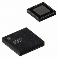
SC16C752BIBS,151 NXP Semiconductors, SC16C752BIBS,151 Datasheet - Page 7

SC16C752BIBS,151
Manufacturer Part Number
SC16C752BIBS,151
Description
IC UART DUAL W/FIFO 32-HVQFN
Manufacturer
NXP Semiconductors
Type
Dual UART with 64-byte FIFOsr
Datasheet
1.SC16C752BIBS151.pdf
(47 pages)
Specifications of SC16C752BIBS,151
Number Of Channels
2, DUART
Package / Case
32-VFQFN Exposed Pad
Features
False-start Bit Detection
Fifo's
64 Byte
Voltage - Supply
2.5V, 3.3V, 5V
With Auto Flow Control
Yes
With False Start Bit Detection
Yes
With Modem Control
Yes
Mounting Type
Surface Mount
Data Rate
5 Mbps
Supply Voltage (max)
5.5 V
Supply Voltage (min)
2.25 V
Supply Current
4.5 mA
Maximum Operating Temperature
+ 85 C
Minimum Operating Temperature
- 40 C
Mounting Style
SMD/SMT
Operating Supply Voltage
2.5 V or 3.3 V or 5 V
Lead Free Status / RoHS Status
Lead free / RoHS Compliant
Lead Free Status / RoHS Status
Lead free / RoHS Compliant, Lead free / RoHS Compliant
Other names
568-3288
935276389151
SC16C752BIBS-S
935276389151
SC16C752BIBS-S
NXP Semiconductors
6. Functional description
SC16C752B
Product data sheet
6.1 Trigger levels
6.2 Hardware flow control
The SC16C752B UART is pin-compatible with the SC16C2550 UART. It provides more
enhanced features. All additional features are provided through a special Enhanced
Feature Register (EFR).
The UART will perform serial-to-parallel conversion on data characters received from
peripheral devices or modems, and parallel-to-parallel conversion on data characters
transmitted by the processor. The complete status of each channel of the SC16C752B
UART can be read at any time during functional operation by the processor.
The SC16C752B can be placed in an alternate mode (FIFO mode) relieving the processor
of excessive software overhead by buffering received/transmitted characters. Both the
receiver and transmitter FIFOs can store up to 64 bytes (including three additional bits of
error status per byte for the receiver FIFO) and have selectable or programmable trigger
levels. Primary outputs RXRDYn and TXRDYn allow signalling of DMA transfers.
The SC16C752B has selectable hardware flow control and software flow control.
Hardware flow control significantly reduces software overhead and increases system
efficiency by automatically controlling serial data flow using the RTSn output and CTSn
input signals. Software flow control automatically controls data flow by using
programmable Xon/Xoff characters.
The UART includes a programmable baud rate generator that can divide the timing
reference clock input by a divisor between 1 and (2
The SC16C752B provides independent selectable and programmable trigger levels for
both receiver and transmitter DMA and interrupt generation. After reset, both transmitter
and receiver FIFOs are disabled and so, in effect, the trigger level is the default value of
one byte. The selectable trigger levels are available via the FIFO Control Register (FCR).
The programmable trigger levels are available via the Trigger Level Register (TLR).
Hardware flow control is comprised of auto-CTS and auto-RTS. Auto-CTS and auto-RTS
can be enabled/disabled independently by programming EFR[7:6].
With auto-CTS, CTSn must be active before the UART can transmit data.
Auto-RTS only activates the RTSn output when there is enough room in the FIFO to
receive data and de-activates the RTSn output when the receive FIFO is sufficiently full.
The halt and resume trigger levels in the TCR determine the levels at which RTSn is
activated/deactivated.
If both auto-CTS and auto-RTS are enabled, when RTSn is connected to CTSn, data
transmission does not occur unless the receiver FIFO has empty space. Thus, overrun
errors are eliminated during hardware flow control. If not enabled, overrun errors occur if
the transmit data rate exceeds the receive FIFO servicing latency.
All information provided in this document is subject to legal disclaimers.
5 V, 2.2 V and 2.5 V dual UART, 5 Mbit/s (max.), with 64-byte FIFOs
Rev. 6 — 30 November 2010
16
− 1).
SC16C752B
© NXP B.V. 2010. All rights reserved.
7 of 47


