SCC2698BC1A84,512 NXP Semiconductors, SCC2698BC1A84,512 Datasheet - Page 5
SCC2698BC1A84,512
Manufacturer Part Number
SCC2698BC1A84,512
Description
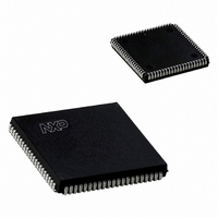
IC UART OCTAL ENHANCED 84-PLCC
Manufacturer
NXP Semiconductors
Type
Octal UARTr
Datasheet
1.SCC2698BC1A84512.pdf
(29 pages)
Specifications of SCC2698BC1A84,512
Number Of Channels
8
Package / Case
84-LCC (J-Lead)
Features
False-start Bit Detection
Fifo's
3Bit
Voltage - Supply
5V
With Auto Flow Control
Yes
With False Start Bit Detection
Yes
With Modem Control
Yes
With Cmos
Yes
Mounting Type
Surface Mount
Data Rate
115.2 Kbps
Supply Voltage (max)
5.25 V
Supply Voltage (min)
4.75 V
Supply Current
30 mA
Maximum Operating Temperature
+ 70 C
Minimum Operating Temperature
0 C
Mounting Style
SMD/SMT
Operating Supply Voltage
5 V
Transmitter And Receiver Fifo Counter
No
Operating Supply Voltage (typ)
5V
Package Type
PLCC
Operating Supply Voltage (max)
5.25V
Operating Supply Voltage (min)
4.75V
Mounting
Surface Mount
Operating Temperature (min)
0C
Operating Temperature (max)
70C
Operating Temperature Classification
Commercial
Lead Free Status / RoHS Status
Lead free / RoHS Compliant
Lead Free Status / RoHS Status
Lead free / RoHS Compliant, Lead free / RoHS Compliant
Other names
568-1120-5
933976250512
SCC2698BC1A84
933976250512
SCC2698BC1A84
Available stocks
Company
Part Number
Manufacturer
Quantity
Price
Company:

Part Number:
SCC2698BC1A84,512
Manufacturer:
NXP Semiconductors
Quantity:
10 000


Philips Semiconductors
PIN DESCRIPTION
2006 Aug 07
D0–D7
CEN
WRN
RDN
A0–A5
RESET
INTRAN–
INTRDN
X1/CLK
X2
RxDa–RxDh
TxDa–TxDh
MPOa–MPOh
MPI0a–MPI0h
Enhanced octal universal asynchronous
receiver/transmitter (Octal UART)
MNEMONIC
MNEMONIC
8–13,
16, 17
18
19
22
23, 25,
27, 29,
31, 32
15
35, 36,
46, 47
7
6
3, 56,
83, 57,
79, 58,
75, 59
1, 41,
81, 49,
74, 52,
73, 55
72, 43,
71, 51,
69, 53,
67, 54
33, 34,
37, 39,
61, 63,
76, 77
PIN
PIN
NO.
TYPE
TYPE
I/O
O
O
O
I
I
I
I
I
I
I
I
I
Data Bus: Active–High 8-bit bidirectional 3-State data bus. Bit 0 is the LSB and bit 7 is the MSB. All
data, command, and status transfers between the CPU and the Octal UART take place over this bus.
The direction of the transfer is controlled by the WRN and RDN inputs when the CEN input is low.
When the CEN input is High, the data bus is in the 3-State condition.
Chip Enable: Active-Low input. When Low, data transfers between the CPU and the Octal UART are
enabled on D0–D7 as controlled by the WRN, RDN and A0–A5 inputs. When CEN is High, the Octal
UART is effectively isolated from the data bus and D0–D7 are placed in the 3-State condition.
Write Strobe: Active-Low input. A Low on this pin while CEN is Low causes the contents of the data
bus to be transferred to the register selected by A0–A5. The transfer occurs on the trailing (rising)
edge of the signal.
Read Strobe: Active-Low input. A Low on this pin while CEN is Low causes the contents of the
register selected by A0–A5 to be placed on the data bus. The read cycle begins on the leading
(falling) edge of RDN.
Address Inputs: Active-High address inputs to select the Octal UART registers for read/write
operations.
Reset: Master reset. A High on this pin clears the status register (SR), clears the interrupt mask
register (IMR), clears the interrupt status register (ISR), clears the output port configuration register
(OPCR), places the receiver and transmitter in the inactive state causing the TxD output to go to the
marking (High) state, and stops the counter/timer. Clears power-down mode and interrupts. Clears
Test Modes, sets MR pointer to MR1.
Interrupt Request: This active-Low open drain output is asserted on occurrence of one or more of
eight maskable interrupting conditions. The CPU can read the interrupt status register to determine
the interrupting condition(s). These pins require a pullup device and may be wire ORed.
Crystal 1: Crystal or external clock input. When using the crystal oscillator, this pin serves as the
connection for one side of the crystal. If a crystal is not used, an external clock is supplied at this
input. An external clock (or crystal) is required even if the internal baud rate generator is not utilized.
This clock is used to drive the internal baud rate generator, as an optional input to the timer/counter,
and to provide other clocking signals required by the chip.
Crystal 2: Connection for other side of crystal. If an external source is used instead of a crystal, this
connection should be left open (see Figure 9).
Receiver Serial Data Input: The least significant bit is received first. If external receiver clock is
specified, this input is sampled on the rising edge of the clock. If internal clock is used, the RxD input
is sampled on the rising edge of the RxC1x signal as seen on the MPO pin.
Transmitter Serial Data Output: The least significant bit is transmitted first. This output is held in the
marking (High) condition when the transmitter is idle or disabled and when the Octal UART is
operating in local loopback mode. If external transmitter is specified, the data is shifted on the falling
edge of the transmitter clock. If internal clock is used, the TxD output changes on the falling edge of
the TxC1x signal as seen on the MPO pin.
Multi-Purpose Output: Each of the four DUARTS has two MPO pins (one per UART). One of the
following eight functions can be selected for this output pin by programming the OPCR (output port
configuration register). Note that reset conditions MPO pins to RTSN.
RTSN – Request to send active-Low output. This output is asserted and negated via the command
register. By appropriate programming of the mode registers, (MR1[7])=1 RTSN can be programmed to
be automatically reset after the character in the transmitter is completely shifted or when the receiver
FIFO and shift register are full. RTSN is an internal signal which normally represents the condition of
the receiver FIFO not full, i.e., the receiver can request more data to be sent. However, it can also be
controlled by the transmitter empty and the commands 8h and 9h written to the CR (command
register).
C/TO – The counter/timer output.
TxC1X – The 1X clock for the transmitter.
TxC16X – The 16X clock for the transmitter.
RxC1X – The 1X clock for the receiver.
RxC16X – The 16X clock for the receiver.
TxRDY – Transmitter holding register empty signal.
RxRDY/FFULL – Receiver FIFO not empty/full signal.
Multi-Purpose Input 0: This pin (one in each UART) is programmable. Its state can always be read
through the IPCR bit 0, or the IPR bit 0.
CTSN: By programming MR2[4] to a 1, this input controls the clear-to-send function for the
transmitter. It is active low. This pin is provided with a change-of-state detector.
5
NAME AND FUNCTION
NAME AND FUNCTION
SCC2698B
Product data sheet
Related parts for SCC2698BC1A84,512
Image
Part Number
Description
Manufacturer
Datasheet
Request
R

Part Number:
Description:
NXP Semiconductors designed the LPC2420/2460 microcontroller around a 16-bit/32-bitARM7TDMI-S CPU core with real-time debug interfaces that include both JTAG andembedded trace
Manufacturer:
NXP Semiconductors
Datasheet:

Part Number:
Description:
NXP Semiconductors designed the LPC2458 microcontroller around a 16-bit/32-bitARM7TDMI-S CPU core with real-time debug interfaces that include both JTAG andembedded trace
Manufacturer:
NXP Semiconductors
Datasheet:
Part Number:
Description:
NXP Semiconductors designed the LPC2468 microcontroller around a 16-bit/32-bitARM7TDMI-S CPU core with real-time debug interfaces that include both JTAG andembedded trace
Manufacturer:
NXP Semiconductors
Datasheet:
Part Number:
Description:
NXP Semiconductors designed the LPC2470 microcontroller, powered by theARM7TDMI-S core, to be a highly integrated microcontroller for a wide range ofapplications that require advanced communications and high quality graphic displays
Manufacturer:
NXP Semiconductors
Datasheet:
Part Number:
Description:
NXP Semiconductors designed the LPC2478 microcontroller, powered by theARM7TDMI-S core, to be a highly integrated microcontroller for a wide range ofapplications that require advanced communications and high quality graphic displays
Manufacturer:
NXP Semiconductors
Datasheet:
Part Number:
Description:
The Philips Semiconductors XA (eXtended Architecture) family of 16-bit single-chip microcontrollers is powerful enough to easily handle the requirements of high performance embedded applications, yet inexpensive enough to compete in the market for hi
Manufacturer:
NXP Semiconductors
Datasheet:
Part Number:
Description:
The XA-S3 device is a member of Philips Semiconductors? XA(eXtended Architecture) family of high performance 16-bitsingle-chip microcontrollers
Manufacturer:
NXP Semiconductors
Datasheet:

Part Number:
Description:
The NXP BlueStreak LH75401/LH75411 family consists of two low-cost 16/32-bit System-on-Chip (SoC) devices
Manufacturer:
NXP Semiconductors
Datasheet:
Part Number:
Description:
The NXP LPC3130/3131 combine an 180 MHz ARM926EJ-S CPU core, high-speed USB2
Manufacturer:
NXP Semiconductors
Datasheet:
Part Number:
Description:
The NXP LPC3141 combine a 270 MHz ARM926EJ-S CPU core, High-speed USB 2
Manufacturer:
NXP Semiconductors
Part Number:
Description:
The NXP LPC3143 combine a 270 MHz ARM926EJ-S CPU core, High-speed USB 2
Manufacturer:
NXP Semiconductors

Part Number:
Description:
The NXP LPC3152 combines an 180 MHz ARM926EJ-S CPU core, High-speed USB 2
Manufacturer:
NXP Semiconductors
Part Number:
Description:
The NXP LPC3154 combines an 180 MHz ARM926EJ-S CPU core, High-speed USB 2
Manufacturer:
NXP Semiconductors

Part Number:
Description:
Standard level N-channel enhancement mode Field-Effect Transistor (FET) in a plastic package using NXP High-Performance Automotive (HPA) TrenchMOS technology
Manufacturer:
NXP Semiconductors
Datasheet: