TDA2050V STMicroelectronics, TDA2050V Datasheet - Page 7
TDA2050V
Manufacturer Part Number
TDA2050V
Description
IC AMP AUDIO PWR HIFI PENTAWATT5
Manufacturer
STMicroelectronics
Type
Class ABr
Datasheet
1.TDA2050V.pdf
(13 pages)
Specifications of TDA2050V
Output Type
1-Channel (Mono)
Max Output Power X Channels @ Load
35W x 1 @ 4 Ohm
Voltage - Supply
9 V ~ 50 V, ±4.5 V ~ 25 V
Features
Short-Circuit and Thermal Protection
Mounting Type
Through Hole
Package / Case
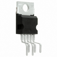
Pentawatt-5 (Vertical, Bent and Staggered Leads)
Product
Class-AB
Output Power
50 W
Available Set Gain
80 dB
Thd Plus Noise
0.03 %
Operating Supply Voltage
25 V
Supply Current
90 mA
Maximum Power Dissipation
25000 mW
Maximum Operating Temperature
+ 150 C
Mounting Style
Through Hole
Audio Load Resistance
8 Ohms
Dual Supply Voltage
+/- 5 V, +/- 9 V, +/- 12 V, +/- 15 V, +/- 18 V, +/- 24 V
Input Bias Current (max)
0.5 uA
Input Offset Voltage
15 mV
Input Signal Type
Differential
Minimum Operating Temperature
- 40 C
Output Signal Type
Single
Supply Type
Dual
Amplifier Class
AB
No. Of Channels
1
Supply Voltage Range
± 4.5V To ± 25V
Load Impedance
4ohm
Operating Temperature Range
-40°C To +150°C
Rohs Compliant
Yes
Lead Free Status / RoHS Status
Lead free / RoHS Compliant
Other names
497-3028-5
Available stocks
Company
Part Number
Manufacturer
Quantity
Price
Company:

Part Number:
TDA2050V
Manufacturer:
MICRON
Quantity:
11 560
Part Number:
TDA2050V
Manufacturer:
ST
Quantity:
20 000


SINGLE SUPPLY APPLICATION SUGGESTIONS
The recommended values of the external compo-
nents are those shown on the application circuit
(*) The gain must be higher than 24dB
NOTE
If the supply voltage is lower than 40V and the
load is 8ohm (or more) a lower value of C2 can
TYPICAL CHARACTERISTICS (Split Supply Test Circuit unless otherwise specified)
Figure 5: Output Power vs. Supply Voltage
Component
R1, R2, R3
R4
R5
R6
C1
C2
C3
C4
C5
C6
C7
Recommended
1000 F
1000 F
0.47 F
100 F
100nF
Value
2.2 F
680
22k
22k
22 F
2.2
Feedback Resistors
Biasing Resistor
Frequency Stability
Input Decoupling DC
Supply Voltage Rejection
Supply Voltage Bypass
Inverting Input DC
Decoupling
Supply Voltage Bypass
Frequency Stability
Output DC Decoupling
Purpose
Increase of Gain
Decrease of Gain (*)
Danger of Oscillations
Worse Turn-off Transient
Worse Turn-on Delay
Increase of Switching
ON/OFF
of fig. 3. Different values can be used. The follow-
ing table can help the designer.
be used (i.e. 22 F).
C7 can be larger than 1000uF only if the supply
voltage does not exceed 40V.
Figure 6: Distortion vs. Output Power
Recommended Value
Larger than
Higher Low-frequency
cut-off
Danger of Oscillations
Worse of Turn-off
Transient
Higher Low-frequency
cut-off
Danger of Oscillations
Danger of Oscillations
Higher Low-frequency
cut-off
Decrease of Gain (*)
Increase of Gain
Recommended Value
Smaller than
TDA2050
7/13
Related parts for TDA2050V
Image
Part Number
Description
Manufacturer
Datasheet
Request
R

Part Number:
Description:
STMicroelectronics [RIPPLE-CARRY BINARY COUNTER/DIVIDERS]
Manufacturer:
STMicroelectronics
Datasheet:
Part Number:
Description:
STMicroelectronics [LIQUID-CRYSTAL DISPLAY DRIVERS]
Manufacturer:
STMicroelectronics
Datasheet:

Part Number:
Description:
BOARD EVAL FOR MEMS SENSORS
Manufacturer:
STMicroelectronics
Datasheet:
Part Number:
Description:
NPN TRANSISTOR POWER MODULE
Manufacturer:
STMicroelectronics
Datasheet:
Part Number:
Description:
TURBOSWITCH ULTRA-FAST HIGH VOLTAGE DIODE
Manufacturer:
STMicroelectronics
Datasheet:
Part Number:
Description:
Manufacturer:
STMicroelectronics
Datasheet:
Part Number:
Description:
DIODE / SCR MODULE
Manufacturer:
STMicroelectronics
Datasheet:
Part Number:
Description:
DIODE / SCR MODULE
Manufacturer:
STMicroelectronics
Datasheet:
Part Number:
Description:
Search -----> STE16N100
Manufacturer:
STMicroelectronics
Datasheet:
Part Number:
Description:
Search ---> STE53NA50
Manufacturer:
STMicroelectronics
Datasheet:
Part Number:
Description:
NPN Transistor Power Module
Manufacturer:
STMicroelectronics
Datasheet:
Part Number:
Description:
DIODE / SCR MODULE
Manufacturer:
STMicroelectronics
Datasheet: