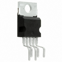
TDA2050V STMicroelectronics, TDA2050V Datasheet - Page 9

TDA2050V
Manufacturer Part Number
TDA2050V
Description
IC AMP AUDIO PWR HIFI PENTAWATT5
Manufacturer
STMicroelectronics
Type
Class ABr
Datasheet
1.TDA2050V.pdf
(13 pages)
Specifications of TDA2050V
Output Type
1-Channel (Mono)
Max Output Power X Channels @ Load
35W x 1 @ 4 Ohm
Voltage - Supply
9 V ~ 50 V, ±4.5 V ~ 25 V
Features
Short-Circuit and Thermal Protection
Mounting Type
Through Hole
Package / Case
Pentawatt-5 (Vertical, Bent and Staggered Leads)
Product
Class-AB
Output Power
50 W
Available Set Gain
80 dB
Thd Plus Noise
0.03 %
Operating Supply Voltage
25 V
Supply Current
90 mA
Maximum Power Dissipation
25000 mW
Maximum Operating Temperature
+ 150 C
Mounting Style
Through Hole
Audio Load Resistance
8 Ohms
Dual Supply Voltage
+/- 5 V, +/- 9 V, +/- 12 V, +/- 15 V, +/- 18 V, +/- 24 V
Input Bias Current (max)
0.5 uA
Input Offset Voltage
15 mV
Input Signal Type
Differential
Minimum Operating Temperature
- 40 C
Output Signal Type
Single
Supply Type
Dual
Amplifier Class
AB
No. Of Channels
1
Supply Voltage Range
± 4.5V To ± 25V
Load Impedance
4ohm
Operating Temperature Range
-40°C To +150°C
Rohs Compliant
Yes
Lead Free Status / RoHS Status
Lead free / RoHS Compliant
Other names
497-3028-5
Available stocks
Company
Part Number
Manufacturer
Quantity
Price
Company:
Part Number:
TDA2050V
Manufacturer:
MICRON
Quantity:
11 560
Part Number:
TDA2050V
Manufacturer:
ST
Quantity:
20 000
Figure 13: Supply Voltage Rejection vs. Fre-
Figure 14: Supply Voltage Rejection vs. Fre-
Figure 15: Total Power Dissipation and Effi-
quency (Single supply) for Different
values of C2 (circuit of fig. 3)
quency (Single supply) for Different
values of C2 (circuit of fig. 3)
ciency vs. Output Power
Figure 16: Total Power Dissipation and Effi-
SHORT CIRCUIT PROTECTION
The TDA 2050 has an original circuit which limits
the current of the output transistors. The maxi-
mum output current is a function of the collector
emitter voltage; hence the output transistors work
within their safe operating area. This function can
therefore be considered as being peak power lim-
iting rather than simple current limiting.
It reduces the possibility that the device gets
damaged during an accidental short circuit from
AC output to ground.
THERMAL SHUTDOWN
The presence of a thermal limiting circuit offers
the following advantages:
The maximum allowable power dissipation de-
pends upon the thermal resistance junction-ambi-
1)An overload on the output (even if it is perma-
2)The heatsink can have a smaller factor of
nent), or an above limit ambient temperature
can be easily tolerated since the Tj cannot be
higher than 150 C.
safety compared with that of a conventional
circuit. There is no possibility of device dam-
age due to high junction temperature. If for
any reason, the junction temperature in-
creases up to 150 C, the thermal shutdown
simply reduces the power dissipation and the
current consumption.
ciency vs. Output Power
TDA2050
9/13


