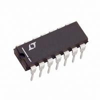
LT1251CN Linear Technology, LT1251CN Datasheet - Page 10

LT1251CN
Manufacturer Part Number
LT1251CN
Description
IC AMP VIDEO FADE CONTRLD 14-DIP
Manufacturer
Linear Technology
Datasheet
1.LT1256CSPBF.pdf
(24 pages)
Specifications of LT1251CN
Applications
Current Feedback
Number Of Circuits
1
-3db Bandwidth
40MHz
Slew Rate
300 V/µs
Current - Supply
14.5mA
Current - Output / Channel
40mA
Voltage - Supply, Single/dual (±)
5 V ~ 30 V, ±2.5 V ~ 15 V
Mounting Type
Through Hole
Package / Case
14-DIP (0.300", 7.62mm)
Lead Free Status / RoHS Status
Contains lead / RoHS non-compliant
Available stocks
Company
Part Number
Manufacturer
Quantity
Price
Part Number:
LT1251CN#PBF
Manufacturer:
LINEAR/凌特
Quantity:
20 000
APPLICATIONS
LT1251/LT1256
Supply Voltage
The LT1251/LT1256 are high speed amplifiers. To prevent
problems, use a ground plane with point-to-point wiring
and small bypass capacitors (0.01 F to 0.1 F) at each
supply pin. For good settling characteristics, especially
driving heavy loads, a 4.7 F tantalum within an inch or two
of each supply pin is recommended.
The LT1251/LT1256 can be operated on single or split
supplies. The minimum total supply is 4V (Pins 7 to 9).
However, the input common mode range is only guaran-
teed to within 2V of each supply. On a 4V supply the parts
must be operated in the inverting mode with the noninvert-
ing input biased half way between Pin 7 and Pin 9. See the
Typical Applications section for the proper biasing for
single supply operation.
The op amps in the control section operate from V
(Pin 7) to within 2V of V
positive supply should be 4.5V or greater in order to use
2.5V control and full-scale voltages.
Inputs
The noninverting inputs (Pins 1 and 14) are easy to drive
since they look like a 17M resistor in parallel with a 1.5pF
capacitor at most frequencies. However, the input stage
can oscillate at very high frequencies (100MHz to 200MHz)
if the source impedance is inductive (like an unterminated
cable). Several inches of wire look inductive at these high
frequencies and can cause oscillations. Check for oscilla-
tions at the inverting inputs (Pins 2 and 13) with a 10
probe and a 200MHz oscilloscope. A small capacitor
(10pF to 50pF) from the input to ground or a small resistor
(100 to 300 ) in series with the input will stop these
parasitic oscillations, even when the source is inductive.
These components must be within an inch of the IC in
order to be effective.
All of the inputs to the LT1251/LT1256 have ESD protec-
tion circuits. During normal operation these circuits have
no effect. If the voltage between the noninverting and
inverting inputs exceeds 6V, the protection circuits will
trigger and attempt to short the inputs together. This
condition will continue until the voltage drops to less than
10
U
INFORMATION
U
+
(Pin 9). For this reason the
W
U
–
500mV or the current to less than 10mA. If a very fast edge
is used to measure settling time with an input step of more
than 6V, the protection circuits will cause the 1mV settling
time to become hundreds of microseconds.
Feedback Resistor Selection
The feedback resistor value determines the bandwidth of
the LT1251/LT1256 as in other current feedback amplifi-
ers. The curves in the Typical Performance Characteristics
show the effect of the feedback resistor on small-signal
bandwidth for various loads, gains and supply voltages.
The bandwidth is limited at high gains by the 500MHz to
800MHz gain-bandwidth product as shown in the curves.
Capacitance on the inverting input will cause peaking and
increase the bandwidth. Take care to minimize the stray
capacitance on Pins 2 and 13 during printed circuit board
layout for flat response.
If the two input stages are not operating with equal gain,
the gain versus control voltage characteristic will be
nonlinear. This is true even if R
because the open-loop characteristic of a current feed-
back amplifier is dependent on the Thevenin impedance at
the inverting input. For linear control of the gain, the loop
gain of the two stages must be equal. For an extreme
example, let’s take a gain of 101 on input 1, R
R
in Figure 1 shows about 25% error at midscale. To
eliminate this nonlinearity we must change the value of
R
inverting input 1 (including the internal resistance of 27 )
times the gain set at input 1. For a linear gain versus
control voltage characteristic when input 2 is operating at
unity-gain, the formula is:
Because the feedback resistor of the unity-gain input is
increased, the bandwidth will be lower and the output
noise will be higher. We can improve this situation by
reducing the values of R
internal 27 dominates.
G1
F2
R
R
. The correct value is the Thevenin impedance at
= 15 , and unity-gain on input 2, R
F2
F2
= (A
= (101)(14.85 + 27) = 4227
V1
)(R
F1
R
G1
F1
+ 27)
and R
G1
F1
, but at high gains the
equals R
F2
= 1.5k. The curve
F1
F2
= 1.5k and
. This is


