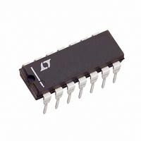
LT1251CN Linear Technology, LT1251CN Datasheet - Page 4

LT1251CN
Manufacturer Part Number
LT1251CN
Description
IC AMP VIDEO FADE CONTRLD 14-DIP
Manufacturer
Linear Technology
Datasheet
1.LT1256CSPBF.pdf
(24 pages)
Specifications of LT1251CN
Applications
Current Feedback
Number Of Circuits
1
-3db Bandwidth
40MHz
Slew Rate
300 V/µs
Current - Supply
14.5mA
Current - Output / Channel
40mA
Voltage - Supply, Single/dual (±)
5 V ~ 30 V, ±2.5 V ~ 15 V
Mounting Type
Through Hole
Package / Case
14-DIP (0.300", 7.62mm)
Lead Free Status / RoHS Status
Contains lead / RoHS non-compliant
Available stocks
Company
Part Number
Manufacturer
Quantity
Price
Part Number:
LT1251CN#PBF
Manufacturer:
LINEAR/凌特
Quantity:
20 000
SIG AL A PLIFIER DC CHARACTERISTICS
CO TROL A D FULL SCALE A PLIFIER CHARACTERISTICS
LT1251/LT1256
0 C T
SYMBOL
A
R
V
I
I
0 C T
SYMBOL
R
R
The
temperature range.
Note 1: A heat sink may be required depending on the power supply
voltage.
Note 2: Commercial grade parts are designed to operate over the
temperature range of – 40 C to 85 C but are neither tested nor guaranteed
beyond 0 C to 70 C. Industrial grade parts specified and tested over
– 40 C to 85 C are available on special request. Consult factory.
Note 3: T
dissipation P
4
O
S
VOL
OL
OUT
C
FS
LT1251CN/LT1256CN:
LT1251CS/LT1256CS:
U
denotes specifications which apply over the specified operating
U
A
A
J
is calculated from the ambient temperature T
Control Amplifier Input Offset Voltage
Full-Scale Amplifier Input Offset Voltage
Control Amplifier Input Resistance
Full-Scale Amplifier Input Resistance
Control Amplifier Input Bias Current
Full-Scale Amplifier Input Bias Current
Internal Control Resistor
Internal Full-Scale Resistor
Resistor Temperature Coefficient
Control Path Bandwidth
Control Path Rise and Fall Time
Control Path Transition Time
Control Path Propagation Delay
PARAMETER
Large-Signal Voltage Gain
Transresistance, V
Maximum Output Voltage Swing
Maximum Output Current
Supply Current
70 C, V
PARAMETER
70 C, V
D
according to the following formulas:
W
S
S
= 5V, V
= 5V, V
U
T
T
J
J
OUT
FS
CM
= T
= T
/ I
= 2.5V, I
A
A
= 0V, V
+ (P
+ (P
IN
–
D
D
• 70 C/W)
• 100 C/W)
FS
C
= I
= 2.5V, I
FS
= NULL = Open, Pins 5,10 = GND, unless otherwise noted.
A
and the power
C
= I
W
FS
= NULL = Open, Pins 5,10 = GND, unless otherwise noted.
CONDITIONS
V
V
V
No Load
V
V
V
V
V
V
V
V
CONDITIONS
Pin 4 to Pin 3
Pin 11 to Pin 12
T
T
Small Signal, V
Small Signal, V
0% to 100%
Small Signal, V
V
V
R
V
A
A
O
O
O
O
L
S
S
S
S
C
C
C
C
C
C
= 25 C
= 25 C
= 15V, No Load
= 5V, V
= 5V
= 5V, V
= V
= V
= V
= V
= V
from 0% or 100%
= – 3V to 3V, R
= – 2.75V to 2.75V, R
= – 3V to 3V, R
= – 2.75V to 2.75V, R
= 150
FS
FS
FS
FS
FS
= 2.5V
= 1.25V
= 0V
= 2.5V, V
= 0V, V
CM
CM
Note 7: Small-signal control path response is measured driving R
to eliminate peaking caused by stray capacitance on Pin 4.
Note 4: Differential gain and phase are measured using a Tektronix
TSG120YC/NTSC signal generator and a Tektronix 1780R Video
Measurement Set. The resolution of this equipment is 0.1% and 0.1 . Five
identical amplifier stages were cascaded giving an effective resolution of
0.02% and 0.02 .
Note 5: Differential gain and phase are best when the control is set at 0%
or 100%. See the Typical Performance Characteristics curves.
Note 6: Tested with R
= 2.5V, (Note 6)
= V
C
C
S
C
= 100mV, (Note 7)
= 100mV, (Note 7)
O
L
L
= 15V
S
= 100mV
= 2.5V
= 150
= 150
= 15V
L
L
= 150
= 150
L
= 150 to 2.5V to simulate an AC coupled load.
– 750
– 750
14.0
0.75
3.75
MIN
MIN
0.75
25
25
83
83
4.0
3.0
2.75
1.2
4
30
20
– 300
– 300
14.2
13.5
14.5
TYP
TYP
100
100
150
0.2
10
35
50
90
93
1.8
4.2
3.5
7.5
1.3
1.4
5
5
5
5
40
30
MAX
17.0
18.5
MAX
6.25
3.8
9.5
1.8
2.0
15
15
6
C
(Pin 5)
UNITS
UNITS
%/ C
MHz
M
M
M
M
mA
mA
mA
mA
mA
mA
mA
mV
mV
k
k
dB
dB
nA
nA
ns
ns
ns
ns
V
V
V
V
V


