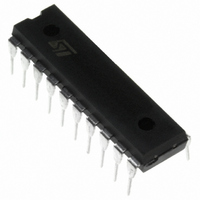
TDA7319 STMicroelectronics, TDA7319 Datasheet

TDA7319
Specifications of TDA7319
Available stocks
Related parts for TDA7319
TDA7319 Summary of contents
Page 1
... ALL FUNCTIONS PROGRAMMABLE VIA SE- 2 RIAL I CBUS DESCRIPTION The TDA7319 is a volume and tone (bass , mid- dle and treble) processor for quality audio appli- cation in car radio and Hi-Fi system. Control is accomplished by serial I processor interface. The AC signal setting is obtained by resistor net- works and switches combined with operational amplifiers ...
Page 2
... TDA7319 ABSOLUTE MAXIMUM RATINGS Symbol V Operating Supply Voltage S T Operating Ambient Temperature amb T Storage Temperature Range stg PIN CONNECTION TREBLE OUT OUT L OUT L THERMAL DATA Symbol R Thermal Resistance Junction-pins th j-amb QUICK REFERENCE DATA Symbol V Supply Voltage S V Max. input signal handling ...
Page 3
... R = 10K ; f = 1KHz; all control = flat ( Test Condition -24dB G = -24 to -47dB -24dB -47dB Adiacent Attenuation Steps From 0dB to A VMAX -24dB G = -24 to -47dB -24dB -47dB Adiacent Attenuation Steps From 0dB to A VMAX d = 0.3% TDA7319 = amb Min. Typ. Max. Unit 0.5 1 ...
Page 4
... The control range -47dB (mute) with a 1dB step. The very high resolution allows the implementation of systems free from any noisy acoustical effect. The TDA7319 audioprocessor provides 3 bands tones control. Bass, Middle Stages The Bass and the middle cells have the same structure ...
Page 5
... Figure 2: Noise vs. volume setting Figure 4: THD vs. frequency Figure 6: Channel separation vs. frequency Figure 3: SVRR vs. frequency Figure 5: THD vs. R LOAD Figure 7: Output clip level vs. Supply voltage TDA7319 5/16 ...
Page 6
... TDA7319 Figure 8: Quiescent current vs. supply voltage Figure 10: Bass response R = 44k C10 = 100nF (Bout, Bin 5.6k Figure 12: Treble response C = 5.6nF TREBLE 6/16 Figure 9: Quiescent current vs. temperature Figure 11: Middle response R = 25k 15nF (MIN 22nF (MOUT 2.7k Figure 13: Typical tone response ...
Page 7
... I C BUS INTERFACE Data transmission from microprocessor to the TDA7319 and viceversa takes place thru the 2 2 wires I C BUS interface, consisting of the two lines SDA and SCL (pull-up resistors to positive supply voltage must be externally connected). Data Validity As shown in fig. 3, the data on the SDA line must be stable during the high period of the clock ...
Page 8
... TDA7319 2 SDA, SCL I CBUS TIMING Symbol f SCL clock frequency SCL t Bus free time between a STOP and START condition BUF t Hold time (repeated) START condition. After this period, the first HD:STA clock pulse is generated t LOW period of the SCL clock LOW t HIGH period of the SCL clock ...
Page 9
... SOFTWARE SPECIFICATION Interface Protocol The interface protocol comprises: A start condition (s) A chip address byte, containing the TDA7319 TDA7319 ADDRESS first byte MSB LSB ACK = Acknowledge S = Start P = Stop MAX CLOCK SPEED 400kbits/s SOFTWARE SPECIFICATION Chip address MSB FUNCTION CODES 1st VOLUME 2nd VOLUME ...
Page 10
... TDA7319 1st VOLUME CODES MSB 2nd VOLUME CODES MSB 10/ LSB FUNCTION 0 step 1dB 0dB -1dB -2dB -3dB -4dB -5dB -6dB -7dB 0 step 8dB 0dB -8dB -16dB -24dB -32dB -40dB MUTE LSB FUNCTION 1 step 1dB 0dB -1dB -2dB -3dB -4dB -5dB -6dB ...
Page 11
... MSB TDA7319 LSB FUNCTION TREBLE BOOST 0 0dB 1 1dB 0 2dB 1 3dB 0 4dB 1 5dB 0 6dB 1 7dB 0 8dB 1 9dB 0 10dB 1 11dB 0 12dB 1 13dB 0 14dB 1 14dB TREBLE CUT 0 0dB 1 -1dB 0 -2dB 1 -3dB 0 -4dB 1 -5dB 0 -6dB 1 -7dB 0 -8dB 1 -9dB 0 -10dB 1 -11dB 0 -12dB 1 -13dB 0 -14dB 1 -14dB 11/16 ...
Page 12
... TDA7319 MIDDLE CODES MSB 12/ LSB FUNCTION MIDDLE BOOST 0 0dB 1 1dB 0 2dB 1 3dB 0 4dB 1 5dB 0 6dB 1 7dB 0 8dB 1 9dB 0 10dB 1 11dB 0 12dB 1 13dB 0 14dB 1 14dB MIDDLE CUT 0 0dB 1 -1dB 0 -2dB 1 -3dB 0 -4dB 1 -5dB 0 -6dB 1 -7dB 0 -8dB 1 -9dB 0 -10dB 1 -11dB 0 -12dB 1 -13dB 0 -14dB ...
Page 13
... TDA7319 LSB FUNCTION BASS BOOST 0 0dB 1 1dB 0 2dB 1 3dB 0 4dB 1 5dB 0 6dB 1 7dB 0 8dB 1 9dB 0 10dB 1 11dB 0 12dB 1 13dB 0 14dB 1 14dB BASS CUT 0 0dB 1 -1dB 0 -2dB 1 -3dB 0 -4dB 1 -5dB 0 -6dB 1 -7dB 0 -8dB 1 -9dB 0 -10dB 1 -11dB 0 -12dB 1 -13dB 0 -14dB 1 -14dB LSB FUNCTION ...
Page 14
... TDA7319 mm DIM. MIN. TYP. MAX. A 2.35 2.65 0.093 A1 0.1 0.3 0.004 B 0.33 0.51 0.013 C 0.23 0.32 0.009 D 12.6 13 0.496 E 7.4 7.6 0.291 e 1. 10.65 0.394 h 0.25 0.75 0.010 L 0.4 1.27 0.016 K 0˚ (min.)8˚ (max 14/16 inch MIN. TYP. MAX. ...
Page 15
... DIM. MIN. TYP. MAX. MIN. a1 0.254 0.010 B 1.39 1.65 0.055 b 0.45 b1 0.25 D 25.4 E 8.5 e 2.54 e3 22.86 F 7.1 I 3.93 L 3.3 Z 1.34 inch MECHANICAL DATA TYP. MAX. 0.065 0.018 0.010 1.000 0.335 0.100 0.900 0.280 0.155 0.130 0.053 TDA7319 OUTLINE AND DIP20 15/16 ...
Page 16
... TDA7319 Information furnished is believed to be accurate and reliable. However, STMicroelectronics assumes no responsibility for the consequences of use of such information nor for any infringement of patents or other rights of third parties which may result from its use. No license is granted by implication or otherwise under any patent or patent rights of STMicroelectronics. Specifications mentioned in this publication are subject to change without notice ...


