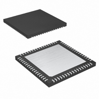
MAX4399CTK+D Maxim Integrated Products, MAX4399CTK+D Datasheet - Page 16

MAX4399CTK+D
Manufacturer Part Number
MAX4399CTK+D
Description
IC SW A/V SCART CON 68-TQFN
Manufacturer
Maxim Integrated Products
Type
Switchr
Datasheet
1.MAX4399CTKTD.pdf
(33 pages)
Specifications of MAX4399CTK+D
Applications
Receivers, Set-Top Boxes, TV
Mounting Type
Surface Mount
Package / Case
68-TQFN Exposed Pad
Lead Free Status / RoHS Status
Lead free / RoHS Compliant
The TV channel incorporates a zero-crossing detect
(ZCD) circuit that minimizes click noise due to abrupt
signal level changes that occur when switching between
audio signals at an arbitrary moment in time.
To implement the zero-cross function when switching
audio signals, set the ZCD bit by loading register 00h
through the I
not already set). Then set the mute bit high by loading
register 00h. Next, wait for a period of time long enough
for the audio signal to cross zero. This period is a func-
tion of the audio signal path’s low frequency 3dB cor-
ner (f
period to wait for zero cross is 1/20Hz or 50ms. Next,
set the appropriate TV switches using register 01h.
Finally, clear the mute bit (while leaving the ZCD bit
high) using register 00h. The MAX4399 switches the
signal out of mute at the next zero crossing.
To implement the zero-cross function for TV volume
changes, or for TV and phono volume bypass switch-
ing, simply ensure the ZCD bit in register 00h is set.
The TV channel volume control ranges from -56dB to
+6dB in 2dB increments. The VCR and AUX volume
control settings are programmable for -6dB, 0dB, and
+6dB. With the ZCD bit set, the TV volume control
switches only at zero crossings, thus minimizing click
noise. The TV outputs can bypass the volume control.
While the phono outputs always follow the TV audio
input selection, the phono outputs can either be
processed through the TV volume control or they can
bypass the TV volume control.
Audio/Video Switch for Three SCART
Connectors
Figure 5. Timing Diagram for SDA and SCL Signals
16
SDA
SCL
______________________________________________________________________________________
L3dB
t
HD
START CONDITION
). For example, if f
,
STA
2
Zero-Cross (Clickless) Switching
C-compatible interface (if the ZCD bit is
t
LOW
t
R
t
SU
t
HIGH
,
L3dB
DAT
t
F
Volume Control
= 20Hz, the time
t
HD
,
DAT
t
SU
REPEATED START CONDITION
,
STA
The MAX4399 uses a simple 2-wire serial interface
requiring only two I/O lines (2-wire bus) of a standard
microprocessor (µP) port. The fast-mode I
ble serial interface allows communication at data rates
up to 400kbps.
signals on the 2-wire bus.
The two bus lines (SDA and SCL) must be high when the
bus is not in use. The MAX4399 is a slave device and
must be controlled by a bus master device. Figure 6
shows a typical application where multiple devices can
be connected to the bus provided they have different
address settings. External pullup resistors are not neces-
sary on these lines (when driven by push-pull drivers),
though the MAX4399 can be used in applications where
pullup resistors are required to maintain compatibility
with existing circuitry. The serial interface operates at
SCL rates up to 400kHz. The SDA state is allowed to
change only while SCL is low, with the exception of
START and STOP conditions as shown in Figure 7.
SDA’s state is sampled, and therefore must remain sta-
ble while SCL is high. Data is transmitted in 8-bit bytes.
Nine clock cycles are required to transfer each byte to
the MAX4399. Release SDA during the 9th clock cycle
as the selected device acknowledges the receipt of the
byte, by pulling SDA low during this time. A series
resistor on the SDA line may be needed if the master’s
output is forced high while the selected device
acknowledges (Figure 6).
t
HD
,
STA
Figure 5 shows the timing diagram for
t
SU
,
STO
STOP CONDITION
Digital Section
Serial Interface
t
BUF
START CONDITION
2
C-compati-


