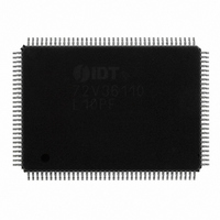
IDT72V36110L10PF IDT, Integrated Device Technology Inc, IDT72V36110L10PF Datasheet - Page 5

IDT72V36110L10PF
Manufacturer Part Number
IDT72V36110L10PF
Description
IC FIFO SYNC 131KX36 10NS 128QFP
Manufacturer
IDT, Integrated Device Technology Inc
Series
72Vr
Datasheet
1.IDT72V36110L7-5BB.pdf
(48 pages)
Specifications of IDT72V36110L10PF
Function
Synchronous
Memory Size
4.7M (131K x 36)
Data Rate
166MHz
Access Time
10ns
Voltage - Supply
3.15 V ~ 3.45 V
Operating Temperature
0°C ~ 70°C
Mounting Type
Surface Mount
Package / Case
128-TQFP, 128-VQFP
Configuration
Dual
Density
4.5Mb
Access Time (max)
6.5ns
Word Size
36b
Organization
128Kx36
Sync/async
Synchronous
Expandable
Yes
Bus Direction
Uni-Directional
Package Type
TQFP
Clock Freq (max)
100MHz
Operating Supply Voltage (typ)
3.3V
Operating Supply Voltage (min)
3.15V
Operating Supply Voltage (max)
3.45V
Supply Current
40mA
Operating Temp Range
0C to 70C
Operating Temperature Classification
Commercial
Mounting
Surface Mount
Pin Count
128
Lead Free Status / RoHS Status
Contains lead / RoHS non-compliant
Other names
72V36110L10PF
800-1530
800-1530
Available stocks
Company
Part Number
Manufacturer
Quantity
Price
Company:
Part Number:
IDT72V36110L10PF
Manufacturer:
IDT, Integrated Device Technology Inc
Quantity:
10 000
Part Number:
IDT72V36110L10PF
Manufacturer:
IDT
Quantity:
20 000
Company:
Part Number:
IDT72V36110L10PF8
Manufacturer:
IDT, Integrated Device Technology Inc
Quantity:
10 000
TABLE 1 — BUS-MATCHING CONFIGURATION MODES
LOW on the LOW-to-HIGH transition of RCLK. PAE is reset to HIGH on the LOW-
to-HIGH transition of WCLK. Similarly, the PAF is asserted LOW on the LOW-
to-HIGH transition of WCLK and PAF is reset to HIGH on the LOW-to-HIGH
transition of RCLK.
updated on the rising edge of RCLK only and not WCLK. Similarly, PAF is
asserted and updated on the rising edge of WCLK only and not RCLK. The mode
desired is configured during Master Reset by the state of the Programmable Flag
Mode (PFM) pin.
once. A LOW on the RT input during a rising RCLK edge initiates a retransmit
operation by setting the read pointer to the first location of the memory array.
A zero-latency retransmit timing mode can be selected using the Retransmit
timing Mode pin (RM). During Master Reset, a LOW on RM will select zero
latency retransmit. A HIGH on RM during Master Reset will select normal
latency.
retransmitted will be placed on the output register with respect to the same RCLK
edge that initiated the retransmit based on RT being LOW.
to Figure 13 and 14 for Zero Latency Retransmit Timing.
shown in Table 1.
useful when data is written into the FIFO in long word format (x36/x18) and read
NOTE:
1. Pin status during Master Reset.
IDT72V36100/72V36110 3.3V HIGH DENSITY SUPERSYNC II
65,536 x 36 and 131,072 x 36
If asynchronous PAE/PAF configuration is selected, the PAE is asserted
If synchronous PAE/PAF configuration is selected , the PAE is asserted and
The Retransmit function allows data to be reread from the FIFO more than
If zero latency retransmit operation is selected, the first data word to be
Refer to Figure 11 and 12 for Retransmit Timing with normal latency. Refer
The device can be configured with different input and output bus widths as
A Big-Endian/Little-Endian data word format is provided. This function is
BM
H
H
H
H
L
IW
H
H
L
L
L
TM
OW
36-BIT FIFO
H
H
L
L
L
5
out of the FIFO in small word (x18/x9) format. If Big-Endian mode is selected,
then the most significant byte (word) of the long word written into the FIFO will
be read out of the FIFO first, followed by the least significant byte. If Little-Endian
format is selected, then the least significant byte of the long word written into the
FIFO will be read out first, followed by the most significant byte. The mode desired
is configured during master reset by the state of the Big-Endian (BE) pin. See
Figure 4 for Bus-Matching Byte Arrangement.
to select the parity bit in the word loaded into the parallel port (D
programming the flag offsets. If Interspersed Parity mode is selected, then the
FIFO will assume that the parity bit is located in bit positions D8, D17, D26 and
D35 during the parallel programming of the flag offsets. If Non-Interspersed
Parity mode is selected, then D8, D17 and D26 are assumed to be valid bits
and D32, D33, D34 and D35 are ignored. IP mode is selected during Master
Reset by the state of the IP input pin. Interspersed Parity control only has an
effect during parallel programming of the offset registers. It does not effect the data
written to and read from the FIFO.
Scan feature, compliant with IEEE 1149.1 Standard Test Access Port and
Boundary Scan Architecture.
automatically power down. Once in the power down state, the standby supply
current consumption is minimized. Initiating any operation (by activating control
inputs) will immediately take the device out of the power down state.
submicron CMOS technology.
The Interspersed/Non-Interspersed Parity (IP) bit function allows the user
A JTAG test port is provided, here the FIFO has fully functional Boundary
If, at any time, the FIFO is not actively performing an operation, the chip will
The IDT72V36100/72V36110 are fabricated using IDT’s high speed
Write Port Width
x36
x36
x36
x18
x9
COMMERCIAL AND INDUSTRIAL
Read Port Width
TEMPERATURE RANGES
OCTOBER 22, 2008
x36
x18
x36
x36
x9
0
-Dn) when


