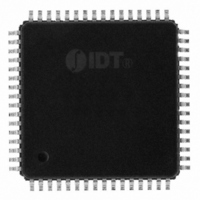
IDT72V271LA10PFG IDT, Integrated Device Technology Inc, IDT72V271LA10PFG Datasheet - Page 5

IDT72V271LA10PFG
Manufacturer Part Number
IDT72V271LA10PFG
Description
IC FIFO SYNC 3.3V 10NS 64-TQFP
Manufacturer
IDT, Integrated Device Technology Inc
Series
72Vr
Datasheet
1.IDT72V271LA10PFG.pdf
(27 pages)
Specifications of IDT72V271LA10PFG
Function
Synchronous
Memory Size
288K (16K x 18)
Access Time
10ns
Voltage - Supply
3 V ~ 3.6 V
Operating Temperature
0°C ~ 70°C
Mounting Type
Surface Mount
Package / Case
64-TQFP, 64-VQFP
Configuration
Dual
Density
288Kb
Access Time (max)
6.5ns
Word Size
9b
Organization
32Kx9
Sync/async
Synchronous
Expandable
Yes
Bus Direction
Uni-Directional
Package Type
TQFP
Clock Freq (max)
100MHz
Operating Supply Voltage (typ)
3.3V
Operating Supply Voltage (min)
3V
Operating Supply Voltage (max)
3.6V
Supply Current
55mA
Operating Temp Range
0C to 70C
Operating Temperature Classification
Commercial
Mounting
Surface Mount
Pin Count
64
Lead Free Status / RoHS Status
Lead free / RoHS Compliant
Data Rate
-
Lead Free Status / Rohs Status
Compliant
Other names
72V271LA10PFG
800-1523
800-1523
Available stocks
Company
Part Number
Manufacturer
Quantity
Price
Company:
Part Number:
IDT72V271LA10PFG
Manufacturer:
IDT, Integrated Device Technology Inc
Quantity:
10 000
Company:
Part Number:
IDT72V271LA10PFG8
Manufacturer:
IDT, Integrated Device Technology Inc
Quantity:
10 000
ABSOLUTE MAXIMUM RATINGS
NOTE:
1. Stresses greater than those listed under ABSOLUTE MAXIMUM RATINGS may cause
NOTES:
1. Industrial temperature range product for 15ns speed grade is available as a standard device. All other speed grades are available by special order.
2. Measurements with 0.4 ≤ V
3. OE ≥ V
4. Tested with outputs disabled (I
5. RCLK and WCLK toggle at 20 MHz and data inputs switch at 10 MHz.
6. Typical I
7. All Inputs = V
CAPACITANCE
NOTES:
1. With output deselected, (OE ≥ V
2. Characterized values, not currently tested.
DC ELECTRICAL CHARACTERISTICS
(Commercial: V
(T
IDT72V261LA/72V271LA
3.3 VOLT CMOS SuperSync FIFO™ 16,384 x 9 and 32,768 x 9
Symbol
C
C
Symbol
I
I
V
V
I
I
permanent damage to the device. This is a stress rating only and functional operation
of the device at these or any other conditions above those indicated in the operational
sections of this specification is not implied. Exposure to absolute maximum rating
conditions for extended periods may affect reliability.
C
Symbol
V
T
I
LI
LO
CC1
CC2
A
IN
OUT
OUT
OH
OL
L
STG
TERM
(2)
= +25°C, f = 1.0MHz)
(3)
(2)
= capacitive load (in pF).
(4,5,6)
(4,7)
(1,2)
IH
CC1
, 0.4 ≤ V
= 10 + 0.95*f
CC
Parameter
Input
Capacitance
Output
Capacitance
Input Leakage Current
Output Leakage Current
Output Logic “1” Voltage, I
Output Logic “0” Voltage, I
Active Power Supply Current
Standby Current
CC
- 0.2V or GND + 0.2V, except RCLK and WCLK, which toggle at 20 MHz.
OUT
Terminal Voltage
with respect to GND
Storage
Temperature
DC Output Current
= 3.3V ± 03.V, TA = 0°C to + 70°C; Industrial: V
≤ V
S
CC
IN
+ 0.02*C
Rating
(1)
.
≤ V
OUT
IH
CC
).
= 0).
.
L
*f
S
Conditions
V
V
IN
OUT
(in mA) with V
= 0V
= 0V
OH
OL
Parameter
= 8 mA
= –2 mA
Com’l & Ind’l
–55 to +125
–50 to +50
–0.5 to +5
CC
= 3.3V, t
Max.
10
10
A
= 25°C, f
mA
Unit
° C
Unit
pF
pF
S
V
= WCLK frequency = RCLK frequency (in MHz, using TTL levels), data switching at f
CC
= 3.3V ± 03.V, TA = -40°C to +85°C)
5
RECOMMENDED DC OPERATING
CONDITIONS
NOTE:
1. 1.5V undershoots are allowed for 10ns once per cycle.
Symbol
GND
V
V
V
T
T
IL
CC
IH
A
A
(1)
Supply Voltage (Com’l/Ind’l)
Supply Voltage (Com’l/Ind’l)
Input High Voltage (Com’l/Ind’l)
Input Low Voltage (Com’l/Ind’l)
Operating Temperature
Commercial
Operating Temperature
Industrial
Min.
–10
2.4
–1
—
—
—
Parameter
Commercial & Industrial
t
CLK
IDT72V261LA
IDT72V271LA
= 10, 15, 20 ns
COMMERCIAL AND INDUSTRIAL
Max.
0.4
TEMPERATURE RANGES
10
55
20
—
Min.
1
(1)
3.0
2.0
-40
⎯
0
0
Typ.
JANUARY 30, 2009
3.3
⎯
⎯
⎯
⎯
0
Max.
+70
+85
3.6
5.0
0.8
S
0
/2,
Unit
mA
mA
µA
µA
V
V
Unit
°C
°C
V
V
V
V


