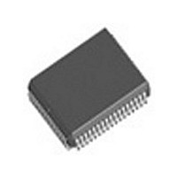
IDT72205LB15JI IDT, Integrated Device Technology Inc, IDT72205LB15JI Datasheet - Page 10

IDT72205LB15JI
Manufacturer Part Number
IDT72205LB15JI
Description
IC FIFO 256X18 SYNC 15NS 68-PLCC
Manufacturer
IDT, Integrated Device Technology Inc
Series
7200r
Datasheet
1.IDT72225LB10PFG.pdf
(16 pages)
Specifications of IDT72205LB15JI
Function
Synchronous
Memory Size
4.6K (256 x 18)
Data Rate
67MHz
Access Time
15ns
Voltage - Supply
4.5 V ~ 5.5 V
Operating Temperature
-40°C ~ 85°C
Mounting Type
Surface Mount
Package / Case
68-PLCC
Configuration
Dual
Density
4.5Kb
Access Time (max)
10ns
Word Size
18b
Organization
256x18
Sync/async
Synchronous
Expandable
Yes
Bus Direction
Uni-Directional
Package Type
PLCC
Clock Freq (max)
66.7MHz
Operating Supply Voltage (typ)
5V
Operating Supply Voltage (min)
4.5V
Operating Supply Voltage (max)
5.5V
Supply Current
60mA
Operating Temp Range
-40C to 85C
Operating Temperature Classification
Industrial
Mounting
Surface Mount
Pin Count
68
Lead Free Status / RoHS Status
Contains lead / RoHS non-compliant
Other names
72205LB15JI
Available stocks
Company
Part Number
Manufacturer
Quantity
Price
NOTE:
1. t
NOTES:
1. When t
2. The first word is available the cycle after EF goes HIGH, always.
IDT72205LB/72215LB/72225LB/72235LB/72245LB CMOS SyncFIFO
256 x 18, 512 x 18, 1,024 x 18, 2,048 x 18 and 4,096 x 18
Q
D
Q
D
edge of RCLK and the rising edge of WCLK is less than t
0
0
WCLK
RCLK
SKEW1
The Latency Timing applies only at the Empty Boundary (EF = LOW).
WCLK
0
0
- Q
RCLK
- D
- Q
- D
17
17
SKEW2
is the minimum time between a rising RCLK edge and a rising WCLK edge to guarantee that FF will go HIGH during the current clock cycle. If the time between the rising
17
17
LOW
DATA IN OUTPUT REGISTER
t
minimum specification, t
ENS
t
ENS
t
SKEW1
t
NO WRITE
DS
(1)
Figure 7. First Data Word Latency after Reset with Simultaneous Read and Write
FRL
D
t
0
(maximum) = t
ENH
(first valid write)
t
A
t
SKEW2
t
WFF
CLK
SKEW1
t
OLZ
+ t
, then FF may not change state until the next WCLK edge.
SKEW2
t
DS
t
FRL
Figure 8. Full Flag Timing
. When t
(1)
D
DATA WRITE
1
t
SKEW2
REF
t
t
ENS
WFF
10
< minimum specification, t
TM
t
DATA READ
OE
t
ENS
D
t
A
t
2
SKEW1
NO WRITE
FRL
(1)
(maximum) = either 2*t
t
ENH
D
t
COMMERCIAL AND INDUSTRIAL
A
0
D
t
A
t
3
TEMPERATURE RANGES
CLK
WFF
NEXT DATA READ
+ t
OCTOBER 22, 2008
SKEW2
t
DS
or t
2766 drw 10
CLK
D
1
2766 drw 09
DATA
WRITE
D
+ t
4
SKEW2
.


