CY7C4291-10JC Cypress Semiconductor Corp, CY7C4291-10JC Datasheet
CY7C4291-10JC
Specifications of CY7C4291-10JC
Available stocks


Related parts for CY7C4291-10JC


CY7C4291-10JC Summary of contents
Page 1
... Features • High-speed, low-power, first-in first-out (FIFO) memories • 64K × 9 (CY7C4281) • 128K × 9 (CY7C4291) • 0.5-micron CMOS for optimum speed/power • High-speed 100-MHz operation (10-ns read/write cycle times) • Low power — — • Fully asynchronous and simultaneous read and write operation • ...
Page 2
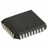
... I When OE is LOW, the FIFO’s data outputs drive the bus to which they are connected HIGH, the FIFO’s outputs are in High Z (high-impedance) state. CY7C4291 128k x 9 32-pin PLCC 7C4281/91-10 100 0.5 8 Commercial 40 Industrial 45 CY7C4281 CY7C4291 Description 7C4281/91-15 7C4281/91-25 66 Page ...
Page 3
... Default Value = 000h Figure 1. Offset Register Location and Default Values CY7C4281 CY7C4291 64K × 9 128K× Empty Offset (LSB) Reg. Empty Offset (LSB) Reg. Default Value = 007h Default Value = 007h 0 8 (MSB) Default Value = 000h ...
Page 4
... The same selection sequence applies to reading from the registers. REN1 and REN2 are enabled and a read is performed on the LOW-to-HIGH transition of RCLK. Document #: 38-06007 Rev greater than or equal to CY7C4281 (64K-m) and CY7C4291 (128K-m). PAF is set HIGH by the LOW-to-HIGH transition of WCLK when the number of available memory locations is greater than m ...
Page 5
... Figure 2. Block Diagram of 64k x 9/128k x 9 Deep Sync FIFO Memory Used in a Width Expansion Configuration Notes Empty Offset ( default value Full Offset ( default value). Document #: 38-06007 Rev. *B RESET (RS) 9 CY7C4281/ Read Enable 2 (REN2) CY7C4281 CY7C4291 READ CLOCK (RCLK) READ ENABLE 1 (REN1) OUTPUT ENABLE (OE) PROGRAMMABLE(PAE) EMPTY FLAG (EF) #1 EMPTY FLAG (EF DATA OUT ( Page ...
Page 6
... Com’l Ind Com’l Ind Description Test Conditions MHz 5.0V CC [9, 10] 3.0V R2 GND 680 1.91V . OHZ CY7C4281 CY7C4291 0. [4] Ambient Temperature + +85 C 7C42X1 10 7C42X1 15 7C42X1 25 Min. Max. Min. Max. Min. 2.4 2.4 2.4 0.4 0.4 2.0 V 2 ...
Page 7
... Almost-Empty Flag and Almost-Full Flag Notes: 11. Pulse widths less than minimum values are not allowed. 12. Values guaranteed by design, not currently tested. Document #: 38-06007 Rev. *B 7C42X1-10 Description Min. 4.5 4.5 0.5 0.5 [12] [12] CY7C4281 CY7C4291 7C42X1-15 7C42X1-25 Max. Min. Max. Min. 100 66 ...
Page 8
... CLKH CLKL t ENH NO OPERATION t REF SKEW1 , then FF may not change state until the next WCLK rising edge. SKEW1 , then EF may not change state until the next RCLK rising edge. SKEW2 CY7C4281 CY7C4291 ENH NO OPERATION NO OPERATION t WFF t REF VALID DATA t OHZ Page ...
Page 9
... Holding WEN2/LD HIGH during reset will make the pin act as a second enable pin. Holding WEN2/LD LOW during reset will make the pin act as a load enable for the programmable flag offset registers. Document #: 38-06007 Rev RSS t RSS t RSS t RSF t RSF t RSF CY7C4281 CY7C4291 t RSR t RSR t RSR [ OE=0 Page ...
Page 10
... The Latency Timing applies only at the Empty Boundary (EF = LOW). 19. The first word is available the cycle after EF goes HIGH, always. Document #: 38-06007 Rev FRL t SKEW1 t REF t OLZ t OE (maximum When t < minimum specification, t CLK SKEW2 SKEW1 CY7C4281 CY7C4291 (maximum) = either 2 FRL CLK SKEW1 Page ...
Page 11
... WEN1 t ENS t t ENS ENH WEN2 (if applicable) t FRL RCLK t SKEW1 EF REN1, REN2 LOW OE DATA IN OUTPUT REGISTER Q – Document #: 38-06007 Rev REF REF t A CY7C4281 CY7C4291 t DS DATA WRITE 2 t ENH t ENS t t ENH ENS [ FRL t t SKEW2 DATA READ REF Page ...
Page 12
... Document #: 38-06007 Rev DATA WRITE t WFF t ENH t A DATA READ t CLKL t t ENS ENH t t ENS ENH Note PAE CY7C4281 CY7C4291 NO WRITE [ SKEW1 t t WFF WFF t ENH t ENS t A NEXT DATA READ WORDS Note 22 IN FIFO ENS ENS ENH DATA WRITE ...
Page 13
... PAF ENS ENH (M+1)WORDS IN FIFO t CLKL t ENH PAE OFFSET PAE OFFSET LSB MSB (m 1) words of the FIFO when PAF goes LOW. m words for CY4291. CY7C4281 CY7C4291 (FULL M) WORDS [ FIFO [ PAF SKEW2 ENS ENS ENH PAF OFFSET PAF OFFSET LSB MSB Page ...
Page 14
... Ordering Information 64K x 9 Deep Sync FIFO Speed (ns) Ordering Code 10 CY7C4281-10JC CY7C4281-10JI 15 CY7C4281-15JC 25 CY7C4281-25JC 128K x 9 Deep Sync FIFO Speed (ns) Ordering Code 10 CY7C4291-10JC CY7C4291-10JI 15 CY7C4291-15JC 25 CY7C4291-25JC Document #: 38-06007 Rev CLKL t ENH t A UNKNOWN PAE OFFSET LSB Package Package Name Type ...
Page 15
... The inclusion of Cypress Semiconductor products in life-support systems application implies that the manufacturer assumes all risk of such use and in doing so indemnifies Cypress Semiconductor against all charges. 32-Lead Plastic Leaded Chip Carrier J65 CY7C4281 CY7C4291 51-85002-*B Page ...
Page 16
... Document History Page Document Title: CY7C4281, CY7C4291 64K/128K X 9 Deep Sync FIFOs Document Number: 38-06007 REV. ECN NO. Issue Date ** 106468 07/12/01 *A 122259 12/26/02 *B 127854 08/22/03 Document #: 38-06007 Rev. *B Orig. of Change SZV Change from Spec number: 38-00587 to 38-06007 RBI Power up requirements added to Operating Range Information ...