CY7C4291-10JC Cypress Semiconductor Corp, CY7C4291-10JC Datasheet - Page 2
CY7C4291-10JC
Manufacturer Part Number
CY7C4291-10JC
Description
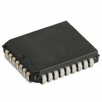
IC DEEP SYNC FIFO 128KX9 32-PLCC
Manufacturer
Cypress Semiconductor Corp
Series
CY7Cr
Datasheet
1.CY7C4291-10JC.pdf
(16 pages)
Specifications of CY7C4291-10JC
Function
Synchronous
Memory Size
1.1M (128K x 9)
Data Rate
100MHz
Access Time
8ns
Voltage - Supply
3.3V
Operating Temperature
-40°C ~ 85°C
Mounting Type
Surface Mount
Package / Case
32-PLCC
Configuration
Dual
Density
1.125Mb
Access Time (max)
8ns
Word Size
9b
Organization
128Kx9
Sync/async
Synchronous
Expandable
Yes
Bus Direction
Uni-Directional
Package Type
PLCC
Clock Freq (max)
100MHz
Operating Supply Voltage (typ)
5V
Operating Supply Voltage (min)
4.5V
Operating Supply Voltage (max)
5.5V
Supply Current
40mA
Operating Temp Range
0C to 70C
Operating Temperature Classification
Commercial
Mounting
Surface Mount
Pin Count
32
Lead Free Status / RoHS Status
Contains lead / RoHS non-compliant
Other names
428-1244
Available stocks
Company
Part Number
Manufacturer
Quantity
Price
Company:

Part Number:
CY7C4291-10JC
Manufacturer:
Cypress Semiconductor Corp
Quantity:
10 000


Document #: 38-06007 Rev. *B
Pin Definitions
Selection Guide
D
Q
WEN1
WEN2/LD
Dual Mode Pin
REN1, REN2
WCLK
RCLK
EF
FF
PAE
PAF
RS
OE
Density
Package
Maximum Frequency
Maximum Access Time
Minimum Cycle Time
Minimum Data or Enable Set-up
Minimum Data or Enable Hold
Maximum Flag Delay
Active Power Supply Current (I
Signal Name
0 – 8
0 8
Data Inputs
Data Outputs
Write Enable 1
Write Enable 2
Load
Read Enable
Inputs
Write Clock
Read Clock
Empty Flag
Full Flag
Programmable
Almost Empty
Programmable
Almost Full
Reset
Output Enable
32-pin PLCC
Description
CY7C4281
64k x 9
CC1
)
I/O
O Data Outputs for 9-bit bus.
O When EF is LOW, the FIFO is empty. EF is synchronized to RCLK.
O When FF is LOW, the FIFO is full. FF is synchronized to WCLK.
O When PAE is LOW, the FIFO is almost empty based on the almost empty offset
O When PAF is LOW, the FIFO is almost full based on the almost full offset value
I
I
I
I
I
I
I
I
Data Inputs for 9-bit bus.
The only write enable when device is configured to have programmable flags.
Data is written on a LOW-to-HIGH transition of WCLK when WEN1 is asserted and FF
is HIGH. If the FIFO is configured to have two write enables, data is written on a
LOW-to-HIGH transition of WCLK when WEN1 is LOW and WEN2/LD and FF are HIGH.
If HIGH at reset, this pin operates as a second write enable. If LOW at reset, this
pin operates as a control to write or read the programmable flag offsets. WEN1 must be
LOW and WEN2 must be HIGH to write data into the FIFO. Data will not be written into
the FIFO if the FF is LOW. If the FIFO is configured to have programmable flags,
WEN2/LD is held LOW to write or read the programmable flag offsets.
Enables the device for Read operation. Both REN1 and REN2 must be asserted to
allow a read operation.
The rising edge clocks data into the FIFO when WEN1 is LOW and WEN2/LD is
HIGH and the FIFO is not Full. When LD is asserted, WCLK writes data into the
programmable flag-offset register.
The rising edge clocks data out of the FIFO when REN1 and REN2 are LOW and
the FIFO is not Empty. When WEN2/LD is LOW, RCLK reads data out of the program-
mable flag-offset register.
value programmed into the FIFO. PAE is synchronized to RCLK.
programmed into the FIFO. PAF is synchronized to WCLK.
Resets device to empty condition. A reset is required before an initial read or write
operation after power-up.
When OE is LOW, the FIFO’s data outputs drive the bus to which they are
connected. If OE is HIGH, the FIFO’s outputs are in High Z (high-impedance) state.
32-pin PLCC
CY7C4291
128k x 9
Commercial
Industrial
7C4281/91-10
100
0.5
10
40
45
8
3
8
Description
7C4281/91-15
66.7
10
15
10
40
4
1
7C4281/91-25
40
15
25
15
40
CY7C4281
CY7C4291
6
1
Page 2 of 16
MHz
Unit
mA
ns
ns
ns
ns
ns
Related parts for CY7C4291-10JC
Image
Part Number
Description
Manufacturer
Datasheet
Request
R

Part Number:
Description:
Manufacturer:
Cypress Semiconductor Corp
Datasheet:

Part Number:
Description:
IC DEEP SYNC FIFO 128KX9 32-PLCC
Manufacturer:
Cypress Semiconductor Corp
Datasheet:
Part Number:
Description:
Manufacturer:
Cypress Semiconductor Corp
Datasheet:
Part Number:
Description:
Manufacturer:
Cypress Semiconductor Corp
Datasheet:
Part Number:
Description:
IC ASYNC FIFO MEM 2KX9 32-PLCC
Manufacturer:
Cypress Semiconductor Corp
Datasheet:
Part Number:
Description:
IC ASYNC FIFO MEM 2KX9 32-PLCC
Manufacturer:
Cypress Semiconductor Corp
Datasheet:
Part Number:
Description:
IC ASYNC FIFO MEM 2KX9 32-PLCC
Manufacturer:
Cypress Semiconductor Corp
Datasheet:
Part Number:
Description:
IC ASYNC FIFO MEM 2KX9 32-PLCC
Manufacturer:
Cypress Semiconductor Corp
Datasheet:
Part Number:
Description:
Manufacturer:
Cypress Semiconductor Corp
Datasheet:
Part Number:
Description:
Manufacturer:
Cypress Semiconductor Corp
Datasheet:
Part Number:
Description:
Manufacturer:
Cypress Semiconductor Corp
Datasheet:
Part Number:
Description:
Manufacturer:
Cypress Semiconductor Corp
Datasheet:
Part Number:
Description:
Manufacturer:
Cypress Semiconductor Corp
Datasheet:
Part Number:
Description:
Manufacturer:
Cypress Semiconductor Corp
Datasheet:
Part Number:
Description:
Manufacturer:
Cypress Semiconductor Corp
Datasheet: