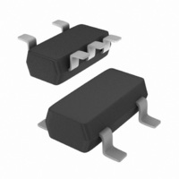
74LVC1G80GV,125 NXP Semiconductors, 74LVC1G80GV,125 Datasheet - Page 5

74LVC1G80GV,125
Manufacturer Part Number
74LVC1G80GV,125
Description
IC SNGL D FF POSEDG TRIG SC74A-5
Manufacturer
NXP Semiconductors
Series
74LVCr
Type
D-Typer
Datasheet
1.74LVC1G80GV125.pdf
(20 pages)
Specifications of 74LVC1G80GV,125
Package / Case
SC-74-5, SOT-753
Function
Standard
Output Type
Inverted
Number Of Elements
1
Number Of Bits Per Element
1
Frequency - Clock
400MHz
Delay Time - Propagation
1.8ns
Trigger Type
Positive Edge
Current - Output High, Low
32mA, 32mA
Voltage - Supply
1.65 V ~ 5.5 V
Operating Temperature
-40°C ~ 125°C
Mounting Type
Surface Mount
Number Of Circuits
1
Logic Family
LVC
Logic Type
D-Type Edge Triggered Flip-Flop
Polarity
Inverting
Input Type
Single-Ended
Propagation Delay Time
2.4 ns at 3.3 V
High Level Output Current
- 32 mA
Supply Voltage (max)
5.5 V
Maximum Operating Temperature
+ 125 C
Mounting Style
SMD/SMT
Minimum Operating Temperature
- 40 C
Supply Voltage (min)
1.65 V
Lead Free Status / RoHS Status
Lead free / RoHS Compliant
Lead Free Status / RoHS Status
Lead free / RoHS Compliant, Lead free / RoHS Compliant
Other names
74LVC1G80GV
74LVC1G80GV
935272023125
74LVC1G80GV
935272023125
NXP Semiconductors
9. Recommended operating conditions
Table 6.
10. Static characteristics
Table 7.
At recommended operating conditions. Voltages are referenced to GND (ground = 0 V).
74LVC1G80
Product data sheet
Symbol
V
V
V
T
Δt/ΔV
Symbol Parameter
T
V
V
V
V
I
I
I
OFF
amb
amb
CC
I
O
IH
IL
OH
OL
= −40 °C to +85 °C
HIGH-level input voltage
LOW-level input voltage
HIGH-level output voltage
LOW-level output voltage
input leakage current
power-off leakage current
Recommended operating conditions
Static characteristics
Parameter
supply voltage
input voltage
output voltage
ambient temperature
input transition rise and fall rate
Conditions
V
V
V
V
V
V
V
V
V
V
V
V
CC
CC
CC
CC
CC
CC
CC
CC
I
I
I
CC
I
I
I
I
I
I
I
I
I
I
I
I
= V
= V
= 5.5 V or GND; V
O
O
O
O
O
O
O
O
O
O
O
O
All information provided in this document is subject to legal disclaimers.
= 1.65 V to 1.95 V
= 2.3 V to 2.7 V
= 2.7 V to 3.6 V
= 4.5 V to 5.5 V
= 1.65 V to 1.95 V
= 2.3 V to 2.7 V
= 2.7 V to 3.6 V
= 4.5 V to 5.5 V
= 0 V; V
= −100 μA; V
= −4 mA; V
= −8 mA; V
= −12 mA; V
= −24 mA; V
= −32 mA; V
= 100 μA; V
= 4 mA; V
= 8 mA; V
= 12 mA; V
= 24 mA; V
= 32 mA; V
IH
IH
Conditions
Active mode
V
V
V
or V
or V
Rev. 9 — 28 September 2010
CC
CC
CC
IL
IL
I
= 0 V; Power-down mode
= 1.65 V to 2.7 V
= 2.7 V to 5.5 V
or V
CC
CC
CC
CC
CC
CC
CC
CC
CC
CC
CC
O
CC
= 1.65 V
= 2.3 V
= 1.65 V
= 2.3 V
= 2.7 V
= 3.0 V
= 4.5 V
= 1.65 V to 5.5 V
= 5.5 V
= 2.7 V
= 3.0 V
= 4.5 V
CC
= 1.65 V to 5.5 V
= 0 V to 5.5 V
Single D-type flip-flop; positive-edge trigger
Min
0.65 × V
1.7
2.0
0.7 × V
-
-
-
-
V
1.2
1.9
2.2
2.3
3.8
-
-
-
-
-
-
-
-
CC
Min
1.65
0
0
0
−40
-
-
− 0.1
CC
CC
Typ
-
-
-
-
-
-
-
74LVC1G80
Typ
-
-
-
-
-
-
-
-
-
-
-
-
-
-
-
-
-
-
-
-
±0.1
±0.1
[1]
© NXP B.V. 2010. All rights reserved.
Max
-
-
-
-
0.35 × V
0.7
0.8
0.3 × V
-
-
-
-
-
-
0.1
0.45
0.3
0.4
0.55
0.55
±5
±10
Max
5.5
5.5
V
5.5
+125
20
10
CC
CC
CC
Unit
V
V
V
V
°C
ns/V
ns/V
5 of 20
Unit
V
V
V
V
V
V
V
V
V
V
V
V
V
V
V
V
V
V
V
V
μA
μA


