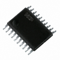
74AHCT574PW,118 NXP Semiconductors, 74AHCT574PW,118 Datasheet - Page 10

74AHCT574PW,118
Manufacturer Part Number
74AHCT574PW,118
Description
IC OCT D FF POS-EDG TRIG 20TSSOP
Manufacturer
NXP Semiconductors
Series
74AHCTr
Type
D-Type Busr
Datasheet
1.74AHC574PW118.pdf
(18 pages)
Specifications of 74AHCT574PW,118
Package / Case
20-TSSOP
Function
Standard
Output Type
Tri-State Non Inverted
Number Of Elements
1
Number Of Bits Per Element
8
Frequency - Clock
115MHz
Delay Time - Propagation
6.3ns
Trigger Type
Positive Edge
Current - Output High, Low
8mA, 8mA
Voltage - Supply
4.5 V ~ 5.5 V
Operating Temperature
-40°C ~ 125°C
Mounting Type
Surface Mount
Number Of Circuits
1
Logic Family
AHCT
Logic Type
D-Type Edge Triggered Flip-Flop
Polarity
Non-Inverting
Input Type
Single-Ended
Propagation Delay Time
4.4 ns
High Level Output Current
- 8 mA
Supply Voltage (max)
5.5 V
Maximum Operating Temperature
+ 125 C
Mounting Style
SMD/SMT
Minimum Operating Temperature
- 40 C
Supply Voltage (min)
4.5 V
Technology
CMOS
Number Of Bits
8
Number Of Elements
1
Clock-edge Trigger Type
Positive-Edge
Operating Supply Voltage (typ)
5V
Package Type
TSSOP
Low Level Output Current
8mA
Frequency (max)
110MHz
Operating Supply Voltage (min)
4.5V
Operating Supply Voltage (max)
5.5V
Operating Temp Range
-40C to 125C
Operating Temperature Classification
Automotive
Mounting
Surface Mount
Pin Count
20
Lead Free Status / RoHS Status
Lead free / RoHS Compliant
Lead Free Status / RoHS Status
Lead free / RoHS Compliant, Lead free / RoHS Compliant
Other names
74AHCT574PW-T
74AHCT574PW-T
935263083118
74AHCT574PW-T
935263083118
Available stocks
Company
Part Number
Manufacturer
Quantity
Price
Company:
Part Number:
74AHCT574PW,118
Manufacturer:
NXP Semiconductors
Quantity:
3 950
NXP Semiconductors
Table 7.
GND = 0 V. For test circuit see
[1]
[2]
[3]
74AHC_AHCT574_2
Product data sheet
Symbol Parameter
t
C
h
Fig 7.
PD
Typical values are measured at nominal supply voltage (V
t
t
t
C
P
f
f
C
V
pd
en
dis
i
o
D
CC
PD
= input frequency in MHz;
L
= output frequency in MHz;
is the same as t
is the same as t
= output load capacitance in pF;
is the same as t
= C
is used to determine the dynamic power dissipation P
= supply voltage in V.
hold time
power
dissipation
capacitance
Measurement points are given in
V
Propagation delay input (CP) to output (Qn), clock input (CP) pulse width and the maximum frequency
(CP)
PD
OL
Dynamic characteristics
and V
V
CC
10.1 Waveforms
2
OH
PLH
PZL
f
PLZ
i
are typical voltage output levels that occur with the output load.
+
Conditions
Dn to CP; see
per buffer;
C
V
and t
and t
and t
I
L
(C
V
C
= GND to V
= 50 pF; f = 1 MHz;
CC
L
L
PZH
PHL
PHZ
= 50 pF
Qn output
CP input
Figure
= 4.5 V to 5.5 V;
V
.
.
.
CC
2
GND
10.
V
f
…continued
V
CC
o
Figure 8
OH
OL
) where:
V
Table
I
8.
Rev. 02 — 24 January 2008
V
M
t
[3]
PHL
t
CC
W
D
Min
( W).
1.5
= 3.3 V and V
-
1/f
V
M
max
Octal D-type flip-flop; positive edge-trigger; 3-state
25 C
Typ
12
-
[1]
74AHC574; 74AHCT574
CC
Max
= 5.0 V).
-
-
t
PLH
40 C to +85 C
Min
1.5
-
mna802
Max
-
-
40 C to +125 C Unit
Min
1.5
-
© NXP B.V. 2008. All rights reserved.
Max
-
-
10 of 18
ns
pF


