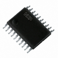
74AHCT574PW,118 NXP Semiconductors, 74AHCT574PW,118 Datasheet - Page 11

74AHCT574PW,118
Manufacturer Part Number
74AHCT574PW,118
Description
IC OCT D FF POS-EDG TRIG 20TSSOP
Manufacturer
NXP Semiconductors
Series
74AHCTr
Type
D-Type Busr
Datasheet
1.74AHC574PW118.pdf
(18 pages)
Specifications of 74AHCT574PW,118
Package / Case
20-TSSOP
Function
Standard
Output Type
Tri-State Non Inverted
Number Of Elements
1
Number Of Bits Per Element
8
Frequency - Clock
115MHz
Delay Time - Propagation
6.3ns
Trigger Type
Positive Edge
Current - Output High, Low
8mA, 8mA
Voltage - Supply
4.5 V ~ 5.5 V
Operating Temperature
-40°C ~ 125°C
Mounting Type
Surface Mount
Number Of Circuits
1
Logic Family
AHCT
Logic Type
D-Type Edge Triggered Flip-Flop
Polarity
Non-Inverting
Input Type
Single-Ended
Propagation Delay Time
4.4 ns
High Level Output Current
- 8 mA
Supply Voltage (max)
5.5 V
Maximum Operating Temperature
+ 125 C
Mounting Style
SMD/SMT
Minimum Operating Temperature
- 40 C
Supply Voltage (min)
4.5 V
Technology
CMOS
Number Of Bits
8
Number Of Elements
1
Clock-edge Trigger Type
Positive-Edge
Operating Supply Voltage (typ)
5V
Package Type
TSSOP
Low Level Output Current
8mA
Frequency (max)
110MHz
Operating Supply Voltage (min)
4.5V
Operating Supply Voltage (max)
5.5V
Operating Temp Range
-40C to 125C
Operating Temperature Classification
Automotive
Mounting
Surface Mount
Pin Count
20
Lead Free Status / RoHS Status
Lead free / RoHS Compliant
Lead Free Status / RoHS Status
Lead free / RoHS Compliant, Lead free / RoHS Compliant
Other names
74AHCT574PW-T
74AHCT574PW-T
935263083118
74AHCT574PW-T
935263083118
Available stocks
Company
Part Number
Manufacturer
Quantity
Price
Company:
Part Number:
74AHCT574PW,118
Manufacturer:
NXP Semiconductors
Quantity:
3 950
NXP Semiconductors
Table 8.
74AHC_AHCT574_2
Product data sheet
Type
74AHC574
74AHCT574
Fig 8.
Fig 9.
Measurement points are given in
V
The shaded areas indicate when the input is permitted to change for predicable output performance.
The data input (D) to clock input (CP) set-up times and clock input (CP) to data input (D) hold times
Measurement points are given in
V
Enable and disable times
OL
OL
Measurement points
and V
and V
OH
OH
are typical voltage output levels that occur with the output load.
are typical voltage output levels that occur with the output load.
HIGH-to-OFF
OFF-to-HIGH
LOW-to-OFF
OFF-to-LOW
Qn output
CP input
Dn input
Qn output
Qn output
OE input
Input
V
0.5V
1.5 V
M
GND
GND
GND
V
GND
V
V
V
V
Table
Table
OH
CC
OL
OH
OL
V
V
V
CC
I
I
I
8.
8.
Rev. 02 — 24 January 2008
V
M
enabled
outputs
V
t
M
PLZ
t
PHZ
V
t
M
su
Output
V
0.5V
0.5V
V
M
X
V
t
Octal D-type flip-flop; positive edge-trigger; 3-state
h
Y
CC
CC
74AHC574; 74AHCT574
V
disabled
outputs
M
t
PZL
t
PZH
t
V
V
V
su
X
OL
OL
V
M
t
+ 0.3 V
+ 0.3 V
h
V
001aah078
M
mna803
outputs
enabled
V
V
V
© NXP B.V. 2008. All rights reserved.
Y
OH
OH
0.3 V
0.3 V
11 of 18


