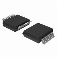
74LV123DB,118 NXP Semiconductors, 74LV123DB,118 Datasheet - Page 5

74LV123DB,118
Manufacturer Part Number
74LV123DB,118
Description
IC DUAL RETRIG MULTIVIB 16SSOP
Manufacturer
NXP Semiconductors
Series
74LVr
Datasheet
1.74LV123N112.pdf
(23 pages)
Specifications of 74LV123DB,118
Logic Type
Monostable
Package / Case
16-SSOP
Independent Circuits
2
Schmitt Trigger Input
Yes
Propagation Delay
14ns
Current - Output High, Low
12mA, 12mA
Voltage - Supply
1 V ~ 5.5 V
Operating Temperature
-40°C ~ 125°C
Mounting Type
Surface Mount
Elements Per Chip
2
Logic Family
LV
Propagation Delay Time
120 ns, 40 ns
High Level Output Current
- 12 mA
Low Level Output Current
12 mA
Supply Voltage (max)
5.5 V
Supply Voltage (min)
1 V
Maximum Operating Temperature
+ 125 C
Minimum Operating Temperature
- 40 C
Mounting Style
SMD/SMT
Operating Supply Voltage
3.3 V
Lead Free Status / RoHS Status
Lead free / RoHS Compliant
Lead Free Status / RoHS Status
Lead free / RoHS Compliant, Lead free / RoHS Compliant
Other names
74LV123DB-T
74LV123DB-T
935210260118
74LV123DB-T
935210260118
NXP Semiconductors
5. Pinning information
74LV123_5
Product data sheet
5.1 Pinning
5.2 Pin description
Table 2.
Symbol
1A
1B
1RD
1Q
2Q
2CEXT
2REXT/CEXT
GND
2A
2B
2RD
2Q
1Q
1CEXT
1REXT/CEXT
V
Fig 5. Pin configuration for DIP16, SO16,
2REXT/CEXT
CC
2CEXT
GND
1RD
SSOP16 and TSSOP16
1Q
2Q
1A
1B
Pin description
1
2
3
4
5
6
7
8
Pin
1
2
3
4
5
6
7
8
9
10
11
12
13
14
15
16
74LV123
Rev. 05 — 8 November 2007
001aag678
Description
negative-edge triggered input 1
positive-edge triggered input 1
direct reset LOW and positive-edge triggered input 1
active LOW output 1
active HIGH output 2
external capacitor connection 2
external resistor and capacitor connection 2
ground (0 V)
negative-edge triggered input 2
positive-edge triggered input 2
direct reset LOW and positive-edge triggered input 2
active LOW output 2
active HIGH output 1
external capacitor connection 1
external resistor and capacitor connection 1
supply voltage
16
15
14
13
12
11
10
9
Dual retriggerable monostable multivibrator with reset
V
1REXT/CEXT
1CEXT
1Q
2Q
2RD
2B
2A
CC
Fig 6. Pin configuration for DHVQFN16
2REXT/CEXT
(1) The die substrate is attached to this
index area
terminal 1
2CEXT
pad using conductive die attach
material. It cannot be used as a
supply pin or input.
1RD
1Q
2Q
1B
Transparent top view
2
3
4
5
6
7
74LV123
V
CC
(1)
© NXP B.V. 2007. All rights reserved.
74LV123
15
14
13
12
11
10
001aag650
1REXT/CEXT
1CEXT
1Q
2Q
2RD
2B
5 of 23


