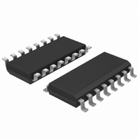
N74F166D,602 NXP Semiconductors, N74F166D,602 Datasheet - Page 6

N74F166D,602
Manufacturer Part Number
N74F166D,602
Description
IC SHIFT REGISTER 8BIT 16-SOIC
Manufacturer
NXP Semiconductors
Series
74Fr
Type
Not Requiredr
Datasheet
1.N74F166N602.pdf
(12 pages)
Specifications of N74F166D,602
Logic Type
Register, Bidirectional
Output Type
Standard
Number Of Elements
1
Number Of Bits Per Element
8
Function
Universal
Voltage - Supply
4.5 V ~ 5.5 V
Operating Temperature
-40°C ~ 85°C
Mounting Type
Surface Mount
Package / Case
16-SOIC (3.9mm Width)
Technology
Bipolar
Number Of Elements
1
Number Of Bits
8
Logic Family
F
Logical Function
Shift Register
Operating Supply Voltage (typ)
5V
Package Type
SOIC W
Propagation Delay Time
12ns
Operating Temp Range
0C to 70C
Operating Supply Voltage (min)
4.5V
Operating Supply Voltage (max)
5.5V
Operating Temperature Classification
Commercial
Mounting
Surface Mount
Pin Count
16
Lead Free Status / RoHS Status
Lead free / RoHS Compliant
Other names
568-3166-5
933802540602
N74F166D
933802540602
N74F166D
1. For conditions shown as MIN or MAX, use the appropriate value specified under recommended operating conditions for the applicable type.
2. All typical values are at V
3. When testing CP, CE must remain in high state, whereas CP must remain in high state when testing CE.
4. Not more than one output should be shorted at a time. For testing I
Philips Semiconductors
DC ELECTRICAL CHARACTERISTICS
(Over recommended operating free-air temperature range unless otherwise noted.)
Notes to DC electrical characteristics
AC ELECTRICAL CHARACTERISTICS
Feb. 14, 1991
SYMBOL
V
V
V
I
I
I
I
I
SYMBOL
f
t
t
t
I
IH
IL
OS
CC
max
PLH
PHL
PHL
8-bit bidirectional universal shift register
techniques are preferable in order to minimize internal heating and more accurately reflect operational values. Otherwise, prolonged shorting
of a high output may raise the chip temperature well above normal and thereby cause invalid readings in other parameter tests. In any
sequence of parameter tests, I
OH
OL
IK
High–level output voltage
Low–level output voltage
Input clamp voltage
Input current at maximum
input voltage
High–level input
current
Low–level input current
Short–circuit output current
Supply current (total)
Maximum clock frequency
Propagation delay
CP to Q7
Propagation delay
MR to Q7
PARAMETER
CC
PARAMETER
= 5V, T
OS
tests should be performed last.
Industrial
amb
only
4
= 25 C.
MR, Ds
others
CONDITION
Waveform 1
Waveform 1
Waveform 2
CE, CP
MR, Ds
MR, Ds
TEST
others
others
others
3
V
MAX,
V
V
MAX,
V
V
V
V
V
V
V
MR = Ds = 4.5V, CP =
CC
IH
CC
IH
CC
CC
CC
CC
CC
CC
MIN
135
5.0
4.0
4.0
= MIN
= MIN
= MIN, V
= MIN, V
= MIN, I
= 0.0V, V
= MAX, V
= MAX, V
= MAX
= MAX, PE = CE = Dn = GND,
T
V
amb
C
R
CC
L
OS
L
6
= 50pF,
= 500
TYP
175
= +25 C
= +5.0V
7.5
6.0
6.5
, the use of high-speed test apparatus and/or sample-and-hold
I
IL
IL
= I
I
I
I
= 7.0V
= 2.7V
= 0.5V
=
=
IK
CONDITIONS
MAX
10.0
8.0
8.5
TEST
I
I
OH
V
OL
CC
MIN
110
5.0
3.5
4.0
T
= MAX
= MAX
amb
C
R
1
= +5.0V
L
L
+70 C
= 50pF,
LIMITS
= 500
= 0 C to
MAX
12.0
10%V
10%V
9.0
9.5
5%V
5%V
10%
CC
CC
CC
CC
T
amb
V
MIN
2.5
2.7
-60
CC
MIN
100
5.0
3.5
4.0
= –40 C to +85 C
C
R
= +5.0V
L
L
LIMITS
= 50pF,
= 500
TYP
-0.73
0.30
0.30
3.4
50
Product specification
2
MAX
74F166
13.0
9.0
9.5
10%
MAX
-150
0.50
0.50
-1.2
100
-20
-40
20
40
40
80
70
UNIT
UNIT
mA
mA
V
V
V
V
V
ns
ns
ns
A
A
A
A
A
A
A


