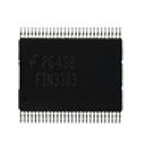
74VCX162839MTDX Fairchild Semiconductor, 74VCX162839MTDX Datasheet - Page 5

74VCX162839MTDX
Manufacturer Part Number
74VCX162839MTDX
Description
IC REGISTER BUFFER 56-TSSOP
Manufacturer
Fairchild Semiconductor
Series
74VCXr
Datasheet
1.74VCX162839MTDX.pdf
(7 pages)
Specifications of 74VCX162839MTDX
Logic Type
Register, Multiplexed
Output Type
Standard
Number Of Elements
1
Number Of Bits Per Element
20
Function
Universal
Voltage - Supply
1.65 V ~ 3.6 V
Operating Temperature
-40°C ~ 85°C
Mounting Type
Surface Mount
Package / Case
56-TSSOP
Logic Family
VCX
Logical Function
Register/Driver
Number Of Elements
1
Number Of Bits
20
Number Of Inputs
20
Number Of Outputs
20
High Level Output Current
-12mA
Low Level Output Current
12mA
Package Type
TSSOP
Propagation Delay Time
9.8ns
Operating Supply Voltage (typ)
1.8/2.5/3.3V
Operating Supply Voltage (max)
3.6V
Operating Supply Voltage (min)
1.65V
Clock-edge Trigger Type
Positive-Edge
Polarity
Non-Inverting
Technology
CMOS
Frequency (max)
250(Min)MHz
Mounting
Surface Mount
Pin Count
56
Operating Temp Range
-40C to 85C
Operating Temperature Classification
Industrial
Quiescent Current
20uA
Lead Free Status / RoHS Status
Lead free / RoHS Compliant
C
C
C
f
t
t
t
t
t
t
t
t
t
t
t
t
t
t
t
t
t
t
t
V
V
V
MAX
PHL
PLH
PHL
PLH
PHL
PZL
PLZ
S
H
W
osHL
osLH
PHL
PHL
PHL
PZL
PLZ
S
H
AC Electrical Characteristics
Note 8: For C
Note 9: Skew is defined as the absolute value of the difference between the actual propagation delay for any two separate outputs of the same device. The
specification applies to any outputs switching in the same direction, either HIGH-to-LOW (t
Extended AC Electrical Characteristics
Note 10: This parameter is guaranteed by characterization but not tested.
Dynamic Switching Characteristics
Capacitance
IN
OUT
PD
Symbol
OLP
OLV
OHV
Symbol
Symbol
Symbol
, t
, t
, t
, t
, t
, t
, t
, t
PZH
PHZ
PZH
PHZ
PLH
PLH
PLH
PLH
Input Capacitance
Output Capacitance
Power Dissipation Capacitance
Maximum Clock Frequency
Propagation Delay I
(REGE
Propagation Delay CLK to O
(REGE
Propagation Delay REGE to O
Output Enable Time
Output Disable Time
Setup Time
Hold Time
Pulse Width
Output to Output Skew
(Note 9)
Propagation Delay I
Propagation Delay CLK to O
Propagation Delay REGE to O
Output Enable Time
Output Disable Time
Setup Time
Hold Time
Quiet Output Dynamic Peak V
Quiet Output Dynamic Valley V
Quiet Output Dynamic Valley V
L
50 pF, add approximately 300 ps to the AC maximum specification.
0)
1)
Parameter
Parameter
n
n
Parameter
to O
to O
n
n
(REGE
Parameter
n
n
(REGE
OL
n
n
OL
OH
0)
1)
V
Min
250
(Note 8)
0.8
0.8
0.8
0.8
0.8
1.0
0.7
1.5
CC
C
C
C
L
L
L
3.3V
30 pF, V
30 pF, V
30 pF, V
V
V
V
V
CC
I
I
CC
T
0V or V
0V or V
Max
0.3V
5
4.3
4.3
A
3.5
4.1
4.9
0.5
IH
IH
IH
1.8V, 2.5V or 3.3V, V
1.8V, 2.5V or 3.3V
Conditions
40 C to 85 C, C
(Note 10)
V
V
V
CC
CC
CC
CC
CC
, V
, f
T
, V
, V
, V
OSHL
A
CC
V
IL
IL
IL
Min
200
1.0
1.0
1.0
1.0
1.0
1.0
0.7
1.5
10 MHz,
CC
) or LOW-to-HIGH (t
Conditions
0 C to 85 C, R
0V
0V
0V
1.8V, 2.5V or 3.3V
2.5V
Min
1.0
1.4
1.0
1.0
1.0
1.0
0.7
I
L
0V or V
Max
0.2V
30 pF, R
4.9
5.8
6.4
6.1
4.9
0.5
C
L
CC
L
OSLH
50 pF
L
500
V
).
500
V
Min
125
CC
1.5
1.5
1.5
1.5
1.5
2.5
1.0
4.0
(V)
1.8
2.5
3.3
1.8
2.5
3.3
1.8
2.5
3.3
CC
V
CC
1.8V
Max
3.8
4.4
5.2
4.6
4.6
www.fairchildsemi.com
T
3.3V
T
A
Typical
A
Typical
0.15V
Max
0.75
0.15
0.25
0.35
1.55
2.05
2.65
9.8
9.8
9.8
9.8
8.8
0.15
0.25
0.35
20
6
7
25 C
25 C
0.3V
Units
Units
MHz
Units
Units
ns
ns
ns
ns
ns
ns
ns
ns
ns
ns
ns
ns
ns
ns
ns
ns
V
V
V
pF
pF
pF


