74LVC257AD,118 NXP Semiconductors, 74LVC257AD,118 Datasheet - Page 2
74LVC257AD,118
Manufacturer Part Number
74LVC257AD,118
Description
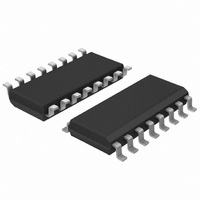
IC QUAD 2-IN MUX 3-ST 16SOIC
Manufacturer
NXP Semiconductors
Series
74LVCr
Type
Multiplexerr
Datasheet
1.74LVC257AD118.pdf
(17 pages)
Specifications of 74LVC257AD,118
Package / Case
16-SOIC (3.9mm Width)
Circuit
4 x 2:1
Independent Circuits
1
Current - Output High, Low
24mA, 24mA
Voltage Supply Source
Single Supply
Voltage - Supply
1.2 V ~ 3.6 V
Operating Temperature
-40°C ~ 125°C
Mounting Type
Surface Mount
Product
Decoders, Encoders, Multiplexers & Demultiplexers
Logic Family
74LVC
Number Of Lines (input / Output)
8.0 / 4.0
Propagation Delay Time
2.9 ns
Supply Voltage (max)
3.6 V
Supply Voltage (min)
1.2 V
Maximum Operating Temperature
+ 125 C
Minimum Operating Temperature
- 40 C
Mounting Style
SMD/SMT
Number Of Input Lines
8.0
Number Of Output Lines
4.0
Power Dissipation
500 mW
Lead Free Status / RoHS Status
Lead free / RoHS Compliant
Lead Free Status / RoHS Status
Lead free / RoHS Compliant, Lead free / RoHS Compliant
Other names
74LVC257AD-T
74LVC257AD-T
935260678118
74LVC257AD-T
935260678118


Philips Semiconductors
FEATURES
QUICK REFERENCE DATA
GND = 0 V; t
Notes
1. C
2. The condition is V
2004 Jan 23
t
t
C
C
t
PZH
PHZ
SYMBOL
PHL
5 V tolerant inputs/outputs, for interfacing with 5 V logic
Wide supply voltage range from 1.2 to 3.6 V
CMOS low-power consumption
Direct interface with TTL levels
Output drive capability 50
Complies with JEDEC standard no. 8-1A
ESD protection:
HBM EIA/JESD22-A114-A exceeds 2000 V
MM EIA/JESD22-A115-A exceeds 200 V
Specified from 40 to +85 C and 40 to +125 C.
I
PD
Quad 2-input multiplexer with 5 V
tolerant inputs/outputs; 3-state
P
f
f
C
V
N = total load switching outputs;
i
o
/t
/t
(C
/t
D
CC
PD
= input frequency in MHz;
L
PZL
PLZ
= output frequency in MHz;
PLH
= output load capacitance in pF;
= C
L
is used to determine the dynamic power dissipation (P
= supply voltage in Volts;
PD
V
CC
r
= t
propagation delay nI0, nI1 to nY
propagation delay S to nY
3-state output enable time OE to nY
3-state output disable time OE to nY
input capacitance
power dissipation capacitance per gate
2
V
f
CC
f
o
2.5 ns; T
2
) = sum of the outputs.
I
f
= GND to V
i
N + (C
amb
PARAMETER
transmission lines at 85 C
= 25 C.
L
CC
.
V
CC
2
f
o
) where:
2
DESCRIPTION
The 74LVC257A is a high-performance, low-power,
low-voltage, Si-gate CMOS device and superior to most
advanced CMOS compatible TTL families.
Inputs can be driven from either 3.3 or 5.0 V devices.
In 3-state operation, outputs can handle 5 V. This feature
allows the use of these devices as translators in a mixed
3.3 and 5 V environment.
The 74LVC257A is a quad 2-input multiplexer with 3-state
outputs, which select 4 bits of data from two sources and
are controlled by a common data select input (pin S). The
data inputs from source 0 (pins 1I0 to 4I0) are selected
when pin S is LOW and the data inputs from source 1
(pins 1I1 to 4I1) are selected when pin S is HIGH. Data
appears at the outputs (pins 1Y to 4Y) in true
(non-inverting) form from the selected inputs. The
74LVC257A is the logic implementation of a 4-pole,
2-position switch, where the position of the switch is
determined by the logic levels applied to pin S. The
outputs are forced to a high-impedance OFF-state when
pin OE is HIGH.
C
C
C
C
V
D
CC
L
L
L
L
outputs enabled
outputs disabled
= 50 pF; V
= 50 pF; V
= 50 pF; V
= 50 pF; V
in W).
= 3.3 V; notes 1 and 2
CONDITIONS
CC
CC
CC
CC
= 3.3 V
= 3.3 V
= 3.3 V
= 3.3 V
2.9
3.2
3.7
3.2
5.0
16
7.0
TYPICAL
Product specification
74LVC257A
ns
ns
ns
ns
pF
pF
pF
UNIT
Related parts for 74LVC257AD,118
Image
Part Number
Description
Manufacturer
Datasheet
Request
R

Part Number:
Description:
NXP Semiconductors designed the LPC2420/2460 microcontroller around a 16-bit/32-bitARM7TDMI-S CPU core with real-time debug interfaces that include both JTAG andembedded trace
Manufacturer:
NXP Semiconductors
Datasheet:

Part Number:
Description:
NXP Semiconductors designed the LPC2458 microcontroller around a 16-bit/32-bitARM7TDMI-S CPU core with real-time debug interfaces that include both JTAG andembedded trace
Manufacturer:
NXP Semiconductors
Datasheet:
Part Number:
Description:
NXP Semiconductors designed the LPC2468 microcontroller around a 16-bit/32-bitARM7TDMI-S CPU core with real-time debug interfaces that include both JTAG andembedded trace
Manufacturer:
NXP Semiconductors
Datasheet:
Part Number:
Description:
NXP Semiconductors designed the LPC2470 microcontroller, powered by theARM7TDMI-S core, to be a highly integrated microcontroller for a wide range ofapplications that require advanced communications and high quality graphic displays
Manufacturer:
NXP Semiconductors
Datasheet:
Part Number:
Description:
NXP Semiconductors designed the LPC2478 microcontroller, powered by theARM7TDMI-S core, to be a highly integrated microcontroller for a wide range ofapplications that require advanced communications and high quality graphic displays
Manufacturer:
NXP Semiconductors
Datasheet:
Part Number:
Description:
The Philips Semiconductors XA (eXtended Architecture) family of 16-bit single-chip microcontrollers is powerful enough to easily handle the requirements of high performance embedded applications, yet inexpensive enough to compete in the market for hi
Manufacturer:
NXP Semiconductors
Datasheet:
Part Number:
Description:
The XA-S3 device is a member of Philips Semiconductors? XA(eXtended Architecture) family of high performance 16-bitsingle-chip microcontrollers
Manufacturer:
NXP Semiconductors
Datasheet:

Part Number:
Description:
The NXP BlueStreak LH75401/LH75411 family consists of two low-cost 16/32-bit System-on-Chip (SoC) devices
Manufacturer:
NXP Semiconductors
Datasheet:
Part Number:
Description:
The NXP LPC3130/3131 combine an 180 MHz ARM926EJ-S CPU core, high-speed USB2
Manufacturer:
NXP Semiconductors
Datasheet:
Part Number:
Description:
The NXP LPC3141 combine a 270 MHz ARM926EJ-S CPU core, High-speed USB 2
Manufacturer:
NXP Semiconductors
Part Number:
Description:
The NXP LPC3143 combine a 270 MHz ARM926EJ-S CPU core, High-speed USB 2
Manufacturer:
NXP Semiconductors

Part Number:
Description:
The NXP LPC3152 combines an 180 MHz ARM926EJ-S CPU core, High-speed USB 2
Manufacturer:
NXP Semiconductors
Part Number:
Description:
The NXP LPC3154 combines an 180 MHz ARM926EJ-S CPU core, High-speed USB 2
Manufacturer:
NXP Semiconductors

Part Number:
Description:
Standard level N-channel enhancement mode Field-Effect Transistor (FET) in a plastic package using NXP High-Performance Automotive (HPA) TrenchMOS technology
Manufacturer:
NXP Semiconductors
Datasheet: