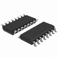
74LVC257AD,118 NXP Semiconductors, 74LVC257AD,118 Datasheet - Page 4

74LVC257AD,118
Manufacturer Part Number
74LVC257AD,118
Description
IC QUAD 2-IN MUX 3-ST 16SOIC
Manufacturer
NXP Semiconductors
Series
74LVCr
Type
Multiplexerr
Datasheet
1.74LVC257AD118.pdf
(17 pages)
Specifications of 74LVC257AD,118
Package / Case
16-SOIC (3.9mm Width)
Circuit
4 x 2:1
Independent Circuits
1
Current - Output High, Low
24mA, 24mA
Voltage Supply Source
Single Supply
Voltage - Supply
1.2 V ~ 3.6 V
Operating Temperature
-40°C ~ 125°C
Mounting Type
Surface Mount
Product
Decoders, Encoders, Multiplexers & Demultiplexers
Logic Family
74LVC
Number Of Lines (input / Output)
8.0 / 4.0
Propagation Delay Time
2.9 ns
Supply Voltage (max)
3.6 V
Supply Voltage (min)
1.2 V
Maximum Operating Temperature
+ 125 C
Minimum Operating Temperature
- 40 C
Mounting Style
SMD/SMT
Number Of Input Lines
8.0
Number Of Output Lines
4.0
Power Dissipation
500 mW
Lead Free Status / RoHS Status
Lead free / RoHS Compliant
Lead Free Status / RoHS Status
Lead free / RoHS Compliant, Lead free / RoHS Compliant
Other names
74LVC257AD-T
74LVC257AD-T
935260678118
74LVC257AD-T
935260678118
Philips Semiconductors
PINNING
2004 Jan 23
handbook, halfpage
Quad 2-input multiplexer with 5 V
tolerant inputs/outputs; 3-state
Fig.1 Pin configuration SO16 and (T)SSOP16.
PIN
10
11
12
13
14
15
16
1
2
3
4
5
6
7
8
9
GND
1I0
1I1
2I0
2I1
1Y
2Y
S
S
1I0
1I1
1Y
2I0
2I1
2Y
GND
3Y
3I1
3I0
4Y
4I1
4I0
OE
V
1
2
3
4
5
6
7
8
CC
SYMBOL
257A
MNA864
15
14
13
12
11
10
16
9
common data select input
data input from source 0
data input from source 1
3-state multiplexer output
data input from source 0
data input from source 1
3-state multiplexer output
ground (0 V)
3-state multiplexer output
data input from source 1
data input from source 0
3-state multiplexer output
data input from source 1
data input from source 0
3-state output enable input (active LOW)
supply voltage
4I0
4I1
4Y
3I0
3I1
3Y
V CC
OE
4
handbook, halfpage
(1) The die substrate is attached to this pad using conductive die
attach material. It can not be used as a supply pin or input.
DESCRIPTION
Fig.2 Pin configuration DHVQFN16.
1I0
1I1
2I0
2I1
1Y
2Y
Top view
2
3
4
5
6
7
GND
S
8
1
GND
V CC
(1)
16
3Y
9
Product specification
MDB198
74LVC257A
15
14
13
12
11
10
OE
4I0
4I1
4Y
3I0
3I1


