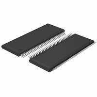
GTL1655DGG,518 NXP Semiconductors, GTL1655DGG,518 Datasheet - Page 11

GTL1655DGG,518
Manufacturer Part Number
GTL1655DGG,518
Description
IC TXRX BUS 16BIT 3-3.6V TSSOP64
Manufacturer
NXP Semiconductors
Datasheet
1.GTL1655DGG518.pdf
(23 pages)
Specifications of GTL1655DGG,518
Logic Function
*
Number Of Bits
16
Input Type
*
Output Type
*
Data Rate
*
Number Of Channels
*
Number Of Outputs/channel
*
Differential - Input:output
*
Propagation Delay (max)
*
Voltage - Supply
3 V ~ 3.6 V
Operating Temperature
-40°C ~ 85°C
Package / Case
64-TSSOP
Mounting Type
Surface Mount
Supply Voltage
3 V ~ 3.6 V
Logic Type
LVTTL-TO-GTL/GTL+ TRANSCEIVER
Logic Family
GTL
Operating Supply Voltage (typ)
3.3V
Propagation Delay Time
7.2ns
Number Of Elements
1
Input Logic Level
LVTTL/TTL
Output Logic Level
GTL
Package Type
TSSOP
Polarity
Non-Inverting
Logical Function
Universal Bus Transceiver
Operating Supply Voltage (min)
3V
Technology
BiCMOS
Operating Temp Range
-40C to 85C
Operating Temperature Classification
Industrial
Mounting
Surface Mount
Pin Count
64
Operating Supply Voltage (max)
3.6V
Lead Free Status / RoHS Status
Lead free / RoHS Compliant
Other names
935270638518
GTL1655DGG-T
GTL1655DGG-T
GTL1655DGG-T
GTL1655DGG-T
Philips Semiconductors
Table 10:
T
[1]
[2]
[3]
[4]
Table 11:
T
9397 750 12936
Product data
Symbol
I
C
C
Symbol
I
(BIAS V
V
I
CC
CC
o
amb
amb
I
o
i
IO
CC
All typical values are measured at V
This is the bus-hold maximum dynamic current. It is the minimum overdrive current required to switch the input from one state to
another.
For I/O ports, this parameter I
This is the increase in supply current for each input that is at the specified TTL voltage level rather than V
= 40 C to +85 C; values otherwise stated V
= 40 C to +85 C
CC
)
DC characteristics
Live insertion characteristics
Parameter
quiescent supply
current
additional quiescent
supply current per input
pin; except port B
input capacitance
I/O capacitance
Parameter
supply current
output voltage
output current
OZ
…continued
includes the input leakage current.
Conditions
V
V
V
V (port B) = 0 to 1.2 V;
V
port B
port B
CC
i
CC
i
CC
(BIAS V
(BIAS V
Conditions
outputs
HIGH
outputs
LOW
disabled
V
V
at V
control pins
port A
port B
= 3.3 V and T
= 0 V to 3.0 V; V (port B) = 0 to 1.2 V;
= 3.0 V to 3.6 V;
CC
CC
CC
= 3.6 V; one input at
0.6 V; port A or control inputs
CC
CC
or GN D
V
V
V
V
V
V (port B) = 0 V to 1.5 V
V
OE = 0 V to 3.3 V;
V (port B) = 0 V to 1.5 V
CC
i
CC
i
CC
CC
) = 3.0 V to 3.6 V
) = 3.0 V to 3.6 V
(BIAS V
(BIAS V
= 0 V;
= 0 V; V (port B) = 0.4 V;
= 0 V to 3.6 V; OE = 3.3 V;
= 0 V to 1.5 V;
REF
amb
Rev. 01 — 11 May 2004
16-bit LVTTL-to-GTL/GTL+ bus transceiver with live insertion
V
V
I
V
V
I
V
V
I
V
V
V
V
V
V
o
o
o
CC
i
CC
i
CC
i
CC
i
CC
i
CC
i
= 25 C.
= 0 mA
= 0 mA
= 0 mA
= V
= V
= V
= V
= V
= V
= 1 V; V
CC
CC
= 3.6 V;
= 3.6 V;
= 3.6 V;
= 3.6 V;
= 3.6 V;
= 3.6 V;
CC
CC
CC
CC
CC
CC
) = 3.3 V
) = 3 V to 3.6 V
or GND;
or GND;
or GND;
or 0
or 0
or 0
TT
= 1.5 V.
[4]
Min
-
-
-
-
-
-
-
Min
-
-
1
-
-
1
© Koninklijke Philips Electronics N.V. 2004. All rights reserved.
Typ
-
-
-
0.1
3
7
8
Typ
-
-
-
-
-
-
[1]
CC
or GND.
GTL1655
Max
45
45
45
-
5
8
10
Max
5
10
1.2
-
300
300
Unit
mA
mA
mA
mA
pF
pF
pF
Unit
mA
V
11 of 23
A
A
A
A


