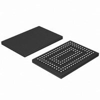
SSTUA32S865ET/G,55 NXP Semiconductors, SSTUA32S865ET/G,55 Datasheet - Page 7

SSTUA32S865ET/G,55
Manufacturer Part Number
SSTUA32S865ET/G,55
Description
IC BUFFER 1.8V 28BIT SOT802
Manufacturer
NXP Semiconductors
Datasheet
1.SSTUA32S865ETG51.pdf
(29 pages)
Specifications of SSTUA32S865ET/G,55
Logic Type
1:2 Registered Buffer with Parity
Supply Voltage
1.7 V ~ 2 V
Number Of Bits
28
Operating Temperature
0°C ~ 70°C
Mounting Type
Surface Mount
Package / Case
160-TFBGA
Lead Free Status / RoHS Status
Lead free / RoHS Compliant
Other names
935279445551
SSTUA32S865ET/G-S
SSTUA32S865ET/G-S
SSTUA32S865ET/G-S
SSTUA32S865ET/G-S
NXP Semiconductors
Table 2.
SSTUA32S865_2
Product data sheet
Symbol
Clock inputs
CK, CK
Miscellaneous inputs
MCL
MCH
RESET
VREF
VDDL
VDDR
GND
n.c.
Pin description
Pin
J1, K1
U3, V2, V3
U5, V5
L1
A1, V1
D4, E4, E6, F4, G4, H4, K4,
K5, N4, N5, P5, P6, R5, R6
E7, F8, F9, G8, G9, J8, J9,
L8, L9, N8, N9, P7, P8
D5, D8, D9, E5, E8, E9, F5,
G5, H5, H8, H9, J4, J5, K8,
K9, L4, L5, M4, M5, M8, M9,
P4, P9, R4, R7, R8, R9
A2, A4, A5, B3, B4, B5, D6,
D7, V4
…continued
Rev. 02 — 16 March 2007
Type
SSTL_18
1.8 V
LVCMOS
0.9 V
nominal
Description
Differential master clock input pair to the register. The
register operation is triggered by a rising edge on the
positive clock input (CK).
Must be connected to a logic LOW.
Must be connected to a logic HIGH.
Asynchronous reset input. When LOW, it causes a reset
of the internal latches, thereby forcing the outputs LOW.
RESET also resets the PTYERR signal.
Input reference voltage for the SSTL_18 inputs. Two pins
(internally tied together) are used for increased reliability.
Power supply voltage.
Power supply voltage.
Ground.
Ball present but not connected to die.
1.8 V DDR2-667 registered buffer with parity
SSTUA32S865
© NXP B.V. 2007. All rights reserved.
7 of 29


