MC14490PG ON Semiconductor, MC14490PG Datasheet - Page 6
MC14490PG
Manufacturer Part Number
MC14490PG
Description
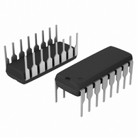
IC ELIMINATOR BOUNCE HEX 16DIP
Manufacturer
ON Semiconductor
Series
4000r
Specifications of MC14490PG
Logic Type
Contact Bounce Eliminator
Supply Voltage
3 V ~ 18 V
Number Of Bits
6
Operating Temperature
-55°C ~ 125°C
Mounting Type
Through Hole
Package / Case
16-DIP (0.300", 7.62mm)
Supply Voltage (max)
18 V
Supply Voltage (min)
3 V
Mounting Style
Through Hole
Number Of Circuits
Hex
Current, Supply
550 μA
Function Type
6-Channels
Logic Function
Bounce Eliminator
Package Type
PDIP-16
Temperature, Operating, Range
-55 to +125 °C
Voltage, Supply
3 to 18 VDC
Logic Case Style
DIP
No. Of Pins
16
Supply Voltage Range
3V To 18V
Operating Temperature Range
-55°C To +125°C
Filter Terminals
DIP
Rohs Compliant
Yes
Clock Frequency Max
4.5MHz
Lead Free Status / RoHS Status
Lead free / RoHS Compliant
Other names
MC14490PGOS
Available stocks
Company
Part Number
Manufacturer
Quantity
Price
Company:

Part Number:
MC14490PG
Manufacturer:
ZORAN
Quantity:
667
Part Number:
MC14490PG
Manufacturer:
ON/安森美
Quantity:
20 000


is that it works with a single signal lead as an input, making
it directly compatible with mechanical contacts (Form A
and B).
The worst case value of the pullup resistor (determined from
the Electrical Characteristics table) is used to calculate the
contact wetting current. If more contact current is required,
an external resistor may be connected between V
input.
be driven with a single standard CMOS gate when V
below 5 V. At this voltage, the input should be driven with
The single most important characteristic of the MC14490
The circuit has a built−in pullup resistor on each input.
Because of the built−in pullup resistors, the inputs cannot
FROM CONTACTS
OSC
OSC
C
ext
CONTACT
“FORM A”
in
out
1
7
9
A
in
CLOCK GENERATOR
+V
OSCILLATOR
TWO-PHASE
OSC
DD
AND
in
MC14490
PULLUP RESISTOR
7
C
Figure 4. Typical “Form A” Contact Debounce Circuit
(INTERNAL)
ext
Figure 5. Typical Single Oscillator Debounce System
9
OSC
1/6 MC14050
out
OPERATING CHARACTERISTICS
φ 1
φ 2
TO SYSTEM
(Only One Debouncer Shown)
LOGIC
DD
and the
http://onsemi.com
DD
4-BIT STATIC SHIFT REGISTER
FROM CONTACTS
is
SHIFT
CONTACTS
6
FROM
paralleled standard gates or by the MC14049 or MC14050
buffers.
such that proper clocking will occur even with very slow
clock edges, eliminating any need for clock preshaping. In
addition, other MC14490 oscillator inputs can be driven
from a single oscillator output buffered by an MC14050 (see
Figure 5). Up to six MC14490s may be driven by a single
buffer.
the outputs. When V
sink 1.6 mA at 0.4 V. The inputs can be driven with TTL as
a result of the internal input pullup resistors.
DATA
The clock input circuit (pin 7) has Schmitt trigger shaping
The MC14490 is TTL compatible on both the inputs and
LOAD
OSC
OSC
in
φ 1 φ 2
7
in
MC14490
MC14490
7
DD
9 OSC
9 OSC
is at 4.5 V, the buffered outputs can
NO CONNECTION
NO CONNECTION
1/2 BIT
DELAY
φ 1 φ 2
out
out
TO SYSTEM
TO SYSTEM
LOGIC
LOGIC
15
A
out
Related parts for MC14490PG
Image
Part Number
Description
Manufacturer
Datasheet
Request
R

Part Number:
Description:
ON Semiconductor [VOLTAGE REGULATOR]
Manufacturer:
ON Semiconductor
Datasheet:
Part Number:
Description:
357-036-542-201 CARDEDGE 36POS DL .156 BLK LOPRO
Manufacturer:
ON Semiconductor
Datasheet:
Part Number:
Description:
357-036-542-201 CARDEDGE 36POS DL .156 BLK LOPRO
Manufacturer:
ON Semiconductor
Datasheet:
Part Number:
Description:
357-036-542-201 CARDEDGE 36POS DL .156 BLK LOPRO
Manufacturer:
ON Semiconductor
Datasheet:
Part Number:
Description:
357-036-542-201 CARDEDGE 36POS DL .156 BLK LOPRO
Manufacturer:
ON Semiconductor
Datasheet:
Part Number:
Description:
357-036-542-201 CARDEDGE 36POS DL .156 BLK LOPRO
Manufacturer:
ON Semiconductor
Datasheet:
Part Number:
Description:
357-036-542-201 CARDEDGE 36POS DL .156 BLK LOPRO
Manufacturer:
ON Semiconductor
Datasheet:
Part Number:
Description:
357-036-542-201 CARDEDGE 36POS DL .156 BLK LOPRO
Manufacturer:
ON Semiconductor
Datasheet:
Part Number:
Description:
357-036-542-201 CARDEDGE 36POS DL .156 BLK LOPRO
Manufacturer:
ON Semiconductor
Datasheet:
Part Number:
Description:
357-036-542-201 CARDEDGE 36POS DL .156 BLK LOPRO
Manufacturer:
ON Semiconductor
Datasheet:
Part Number:
Description:
357-036-542-201 CARDEDGE 36POS DL .156 BLK LOPRO
Manufacturer:
ON Semiconductor
Datasheet:
Part Number:
Description:
Manufacturer:
ON Semiconductor
Datasheet:
Part Number:
Description:
Manufacturer:
ON Semiconductor
Datasheet:
Part Number:
Description:
Manufacturer:
ON Semiconductor
Datasheet: