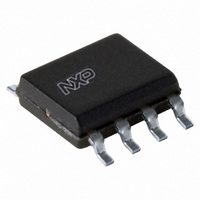
PCA9306D,118 NXP Semiconductors, PCA9306D,118 Datasheet - Page 8

PCA9306D,118
Manufacturer Part Number
PCA9306D,118
Description
IC LEVEL TRANSLATOR 8-SOIC
Manufacturer
NXP Semiconductors
Datasheet
1.PCA9306DP118.pdf
(26 pages)
Specifications of PCA9306D,118
Package / Case
8-SOIC (3.9mm Width)
Logic Function
Translator, Bidirectional, Open Drain
Number Of Bits
2
Input Type
Voltage
Output Type
Voltage
Number Of Channels
2
Number Of Outputs/channel
1
Differential - Input:output
No/No
Voltage - Supply
1 V ~ 3.6 V, 1.8 V ~ 5.5 V
Operating Temperature
-40°C ~ 85°C
Supply Voltage
1.2 V ~ 5.5 V
Supply Voltage (max)
5 V
Supply Voltage (min)
0 V
Maximum Operating Temperature
+ 85 C
Minimum Operating Temperature
- 40 C
Mounting Style
SMD/SMT
Lead Free Status / RoHS Status
Lead free / RoHS Compliant
Data Rate
-
Lead Free Status / Rohs Status
Lead free / RoHS Compliant
Other names
568-4215-2
935283119118
PCA9306D-T
PCA9306D-T
935283119118
PCA9306D-T
PCA9306D-T
NXP Semiconductors
10. Dynamic characteristics
Table 7.
T
Table 8.
T
PCA9306
Product data sheet
Symbol
V
t
t
V
t
t
Symbol
V
t
t
V
t
t
PLH
PHL
PLH
PHL
PLH
PHL
PLH
PHL
amb
amb
Fig 10. Load circuit for outputs
I(EN)
I(EN)
I(EN)
I(EN)
=
=
= 3.3 V; V
= 2.5 V; V
= 3.3 V; V
= 2.5 V; V
a. Load circuit
−
−
40
40
S1 = translating up; S2 = translating down.
C
All input pulses are supplied by generators having the following characteristics: PRR ≤ 10 MHz; Z
The outputs are measured one at a time, with one transition per measurement.
°
°
Parameter
LOW to HIGH
propagation delay
HIGH to LOW
propagation delay
LOW to HIGH
propagation delay
HIGH to LOW
propagation delay
Parameter
LOW to HIGH
propagation delay
HIGH to LOW
propagation delay
LOW to HIGH
propagation delay
HIGH to LOW
propagation delay
L
Dynamic characteristics (translating down)
Dynamic characteristics (translating up)
C to +85
C to +85
from output under test
includes probe and jig capacitance.
IH
IH
IH
IH
= 3.3 V; V
= 2.5 V; V
= 2.3 V; V
= 1.5 V; V
°
°
C, unless otherwise specified. Values guaranteed by design.
C, unless otherwise specified. Values guaranteed by design.
IL
IL
IL
IL
= 0 V; V
= 0 V; V
= 0 V; V
= 0 V; V
Conditions
from (input) SCL2 or SDA2
to (output) SCL1 or SDA1
from (input) SCL2 or SDA2
to (output) SCL1 or SDA1
from (input) SCL2 or SDA2
to (output) SCL1 or SDA1
from (input) SCL2 or SDA2
to (output) SCL1 or SDA1
Conditions
from (input) SCL1 or SDA1
to (output) SCL2 or SDA2
from (input) SCL1 or SDA1
to (output) SCL2 or SDA2
from (input) SCL1 or SDA1
to (output) SCL2 or SDA2
from (input) SCL1 or SDA1
to (output) SCL2 or SDA2
C L
M
M
TT
TT
V
= 1.15 V (see
= 0.75 V (see
002aab845
= 3.3 V; V
= 2.5 V; V
TT
All information provided in this document is subject to legal disclaimers.
S1
S2 (open)
R L
Rev. 6 — 25 November 2010
Dual bidirectional I
M
M
= 1.15 V; R
= 0.75 V; R
Figure
Figure
10)
10)
L
L
= 300 Ω (see
= 300 Ω (see
Min
Min
b. Timing diagram
C
C
0
0
0
0
0
0
0
0
output
L
L
input
= 50 pF
= 50 pF
2
C-bus and SMBus voltage-level translator
Max
Max
1.75
2.75
1.75
2.0
2.0
2.0
2.5
3.3
Figure
Figure
V
V
M
M
Min
Min
C
C
0
0
0
0
0
0
0
0
L
L
10)
10)
= 30 pF
= 30 pF
Max
Max
1.65
1.2
1.5
1.2
1.5
1.0
1.0
2.0
o
= 50 Ω; t
V
V
M
M
Min
Min
PCA9306
C
C
0
0
0
0
0
0
0
0
© NXP B.V. 2010. All rights reserved.
L
L
002aab846
r
= 15 pF
= 15 pF
≤ 2 ns; t
Max
0.75
0.75
Max
0.6
0.6
0.5
0.8
0.5
1.0
V
V
V
V
IH
IL
OH
OL
f
≤ 2 ns.
Unit
ns
ns
ns
ns
Unit
ns
ns
ns
ns
8 of 26


