ADG3123BRUZ Analog Devices Inc, ADG3123BRUZ Datasheet
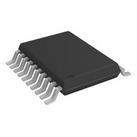
IC XLATOR 8CH LOG-HV 20-TSSOP

ADG3123BRUZ

Manufacturer Part Number
ADG3123BRUZ
Description
IC XLATOR 8CH LOG-HV 20-TSSOP
Manufacturer
Analog Devices Inc
Datasheet

Specifications of ADG3123BRUZ

Logic Function
Translator
Number Of Bits
8
Input Type
CMOS
Output Type
Voltage
Number Of Channels
8
Number Of Outputs/channel
1
Differential - Input:output
No/No
Propagation Delay (max)
125ns
Voltage - Supply
2.3 V ~ 5.5 V
Operating Temperature
-40°C ~ 85°C
Package / Case
20-TSSOP
Supply Voltage
2.3 V ~ 5.5 V
No. Of Inputs
8
Propagation Delay
76ns
Logic Type
Level Translator
Supply Voltage Range
2.3V To 5.5V
Logic Case Style
TSSOP
No. Of Pins
20
Operating Temperature Range
-40°C To +85°C
Lead Free Status / RoHS Status
Lead free / RoHS Compliant
Data Rate
-
Lead Free Status / RoHS Status
Lead free / RoHS Compliant, Lead free / RoHS Compliant

Available stocks

Company
Part Number
Manufacturer
Quantity
Price
Part Number:
ADG3123BRUZ
Manufacturer:
Analog Devices Inc
Quantity:
1 970
Part Number:
ADG3123BRUZ
Manufacturer:
ADI/亚德诺
Quantity:
20 000
FEATURES
2.3 V to 5.5 V input voltage range
Output voltage levels (V
Rise/fall time: 12 ns/19.5 ns typical
Propagation delay: 80 ns typical
Operating frequency: 100 kHz typical
Ultralow quiescent current: 65 μA typical
20-lead, Pb-free, TSSOP package
APPLICATIONS
Low voltage to high voltage translation
TFT-LCD panels
Piezoelectric motor drivers
GENERAL DESCRIPTION
The ADG3123 is an 8-channel, noninverting CMOS to high
voltage level translator. Fabricated on an enhanced LC
process, the device is capable of operating at high supply
voltages while maintaining ultralow power consumption.
The internal architecture of the device ensures compatibility
with logic circuits running from supply voltages within the 2.3 V to
5.5 V range. The voltages applied to Pin V
Pin V
of the device. Pin V
for Pin Y1 to Pin Y6 and for Pin Y7 to Pin Y8, respectively. The
V
can provide output voltages levels down to −10 V for a low
input level and up to +30 V for a high input logic level. For
proper operation, V
V
not exceed 35 V.
The low output impedance of the channels guarantees fast rise
and fall times even for significant capacitive loads. This feature,
combined with low propagation delay and low power consump-
tion, makes the ADG3123 an ideal driver for TFT-LCD panel
applications.
Rev. A
Information furnished by Analog Devices is believed to be accurate and reliable. However, no
responsibility is assumed by Analog Devices for its use, nor for any infringements of patents or other
rights of third parties that may result from its use. Specifications subject to change without notice. No
license is granted by implication or otherwise under any patent or patent rights of Analog Devices.
Trademarks and registered trademarks are the property of their respective owners.
SS
DDA
Low output voltage levels: down to −24.4 V
High output voltage levels: up to +35 V
pin sets the low output level for all channels. The ADG3123
and the voltage between the Pin V
SS
set the logic levels available at the outputs on the Y side
DDA
DDB
and Pin V
must always be greater than or equal to
DDA
and V
DDB
DDB
set the high output level
to V
DDB
DDA
SS
and Pin V
≤ 35 V)
, Pin V
DDB,
SS
2
MOS
should
8-Channel CMOS Logic to High Voltage
and
One Technology Way, P.O. Box 9106, Norwood, MA 02062-9106, U.S.A.
Tel: 781.329.4700
Fax: 781.461.3113
The ADG3123 is guaranteed to operate over the −40°C to
+85°C temperature range and is available in a compact, 20-lead
TSSOP, Pb-free package.
PRODUCT HIGHLIGHTS
1.
2.
3.
4.
5.
Compatible with a wide range of CMOS logic levels.
High output voltage levels.
Fast rise and fall times coupled with low propagation delay.
Ultralow power consumption.
Compact, 20-lead TSSOP, Pb-free package.
FUNCTIONAL BLOCK DIAGRAM
GND
A1
A2
A3
A4
A5
A6
A7
A8
©2006 Analog Devices, Inc. All rights reserved.
CHANNELS
CHANNELS
V
V
DDA
DDB
6
2
Figure 1.
Level Translator
ADG3123
ADG3123
Y1
Y2
Y3
Y4
Y5
Y6
V
Y7
Y8
www.analog.com
SS

Related parts for ADG3123BRUZ

ADG3123BRUZ Summary of contents

Page 1

FEATURES 2 5.5 V input voltage range Output voltage levels (V and DDA DDB Low output voltage levels: down to −24.4 V High output voltage levels +35 V Rise/fall time: 12 ns/19.5 ns ...

Page 2

ADG3123 TABLE OF CONTENTS Features .............................................................................................. 1 Applications....................................................................................... 1 Functional Block Diagram .............................................................. 1 General Description ......................................................................... 1 Product Highlights ........................................................................... 1 Revision History ............................................................................... 2 Specifications..................................................................................... 3 Absolute Maximum Ratings............................................................ 4 ESD Caution.................................................................................. 4 Pin Configuration and Function Descriptions............................. ...

Page 3

SPECIFICATIONS −7 V, GND = 0 V, unless otherwise noted. DDA DDB SS Table 1. Parameter DIGITAL INPUTS (Pin A1 to Pin A8) Input High Voltage Input Low Voltage Leakage Current 3 ...

Page 4

ADG3123 ABSOLUTE MAXIMUM RATINGS T = 25°C, unless otherwise noted. A Table 2. Parameter Rating DDA DDB GND −0 +32 V DDB V to GND −0 ...

Page 5

PIN CONFIGURATION AND FUNCTION DESCRIPTIONS Table 3. Pin Function Descriptions Pin No. Mnemonic Description 1 GND Ground Reference (0 V Level Translator CMOS Inputs Most Negative Power Supply. Use the V SS ...

Page 6

ADG3123 TYPICAL PERFORMANCE CHARACTERISTICS 4 25° – 5kΩ 100pF L DUTY CYCLE = 50% 3.7 1 CHANNEL 3.5 DDA 3.3 3 DDA ...

Page 7

T = 25° 27V DDA DDB V = –7V SS 250 R = 5kΩ L FREQUENCY = 20kHz DUTY CYCLE = 50% 200 1 CHANNEL 150 100 50 0 0.10 0.60 1.10 1.60 2.10 ...

Page 8

ADG3123 –6 ° 27V DDA DDB V = – CHANNEL –6.6 –6.8 –7 LOAD CURRENT (mA) Figure 16. Output Voltage (V ) vs. ...

Page 9

TERMINOLOGY V IH Logic input high voltage at Pin A1 to Pin A8 Logic input low voltage at Pin A1 to Pin A8 Leakage current at Pin A1 to Pin A8 Capacitance measured at ...

Page 10

ADG3123 THEORY OF OPERATION The ADG3123 is an 8-channel, noninverting CMOS to high voltage level translator. Fabricated on an enhanced LC process, the device is capable of operating at high supply voltages while maintaining ultralow power consumption. The device requires ...

Page 11

APPLICATIONS The high voltage operation coupled with high current driving capability and the wide range of CMOS levels accepted by the ADG3123, make the device ideal for LCD-TFT panel applica- tions. In this type of application, the controllers that generate ...

Page 12

... ORDERING GUIDE Model Temperature Range 1 ADG3123BRUZ −40°C to +85°C 1 ADG3123BRUZ-REEL −40°C to +85°C 1 ADG3123BRUZ-REEL7 −40°C to +85° Pb-free part. ©2006 Analog Devices, Inc. All rights reserved. Trademarks and registered trademarks are the property of their respective owners. 6.60 6.50 6. ...

Related keywords